Datasheet4U Logo Datasheet4U.com

MTV20N50E - TMOS POWER FET

Key Features

  • e resistance of the driving source, but the internal resistance is difficult to measure and, consequently, is not specified. The resistive switching time variation versus gate resistance (Figure 9) shows how typical switching performance is affected by the parasitic circuit elements. If the parasitics were not present, the slope of the curves would maintain a value of unity regardless of the switching speed. The circuit used to obtain the data is constructed to minimize common inductance in the.

📥 Download Datasheet

Full PDF Text Transcription (Reference)

The following content is an automatically extracted verbatim text from the original manufacturer datasheet and is provided for reference purposes only.

View original datasheet text
MOTOROLA SEMICONDUCTOR TECHNICAL DATA Order this document by MTV20N50E/D ™ Data Sheet TMOS E-FET.™ Power Field Effect Transistor D3PAK for Surface Mount Designer's MTV20N50E 
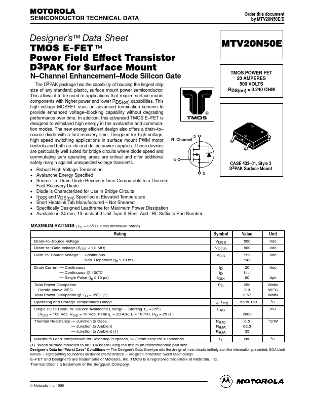
TMOS POWER FET 20 AMPERES 500 VOLTS RDS(on) = 0.240 OHM N–Channel Enhancement–Mode Silicon Gate The D3PAK package has the capability of housing the largest chip size of any standard, plastic, surface mount power semiconductor. This allows it to be used in applications that require surface mount components with higher power and lower RDS(on) capabilities. This high voltage MOSFET uses an advanced termination scheme to provide enhanced voltage–blocking capability without degrading performance over time. In addition, this advanced TMOS E–FET is designed to withstand high energy in the avalanche and commutation modes.