Motorola TL062
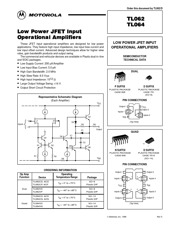
LOW POWER JFET INPUT OPERATIONAL AMPLIFIERS
| Part No. | TL062 |
|---|---|
| Datasheet | TL062 Download |
| Manufacturer |  Motorola |
| Description | LOW POWER JFET INPUT OPERATIONAL AMPLIFIERS |
| Buy | Stock & Price |
MAXIMUM RATINGS
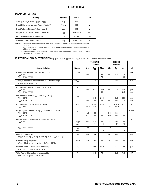
Rating Supply Voltage (from VCC to VEE) Input Differential Voltage Range (Note 1) Input Voltage Range (Notes 1 and 2) Output Short Circuit Duration (Note 3) Operating Junction Temperature Storage Temperature Range Symbol VS VIDR VIR tSC TJ Tstg Value +36 ±30 ±15 Indefinite +150 –60 to +150 Unit V V V sec °C °C NOTES: 1. Differential voltages are at the noninverting input terminal with respect to the inverting input terminal. 2. The magnitude of the input voltage must never exceed the magnitude of the supply or 15 V, whichever is less. 3. Power dissipation must be considered to ensure maximum junction temperature (TJ) is not exceeded. (See Figure 1.)ELECTRICAL CHARACTERISTICS
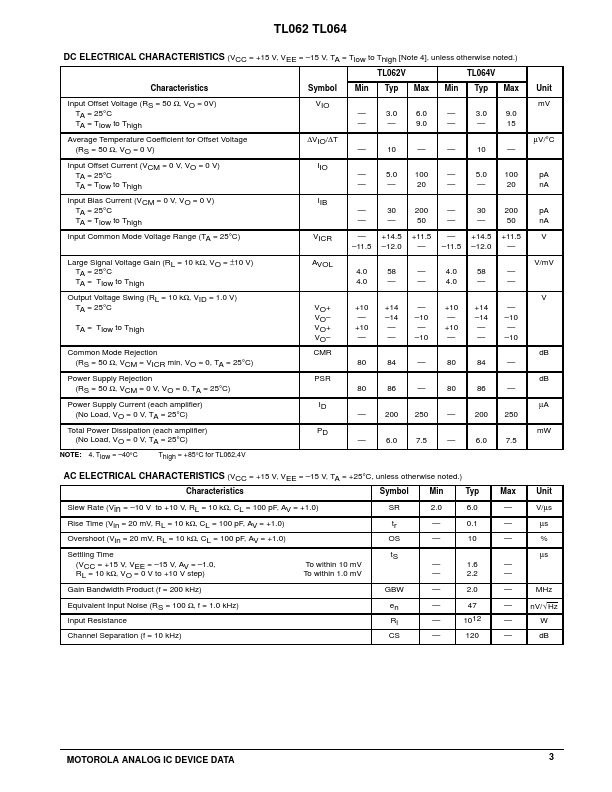
(VCC = +15 V, VEE = –15 V, TA = 0° to +70°C, unless otherwise noted.) TL062AC TL064AC Characteristics Input Offset Voltage (RS = 50 Ω, VO = 0V) TA = 25°C TA = 0° to +70°C Average Temperature Coefficient for Offset Voltage (RS = 50 Ω, VO = 0 V) Input Offset Current (VCM = 0 V, VO = 0 V) TA = 25°C TA...