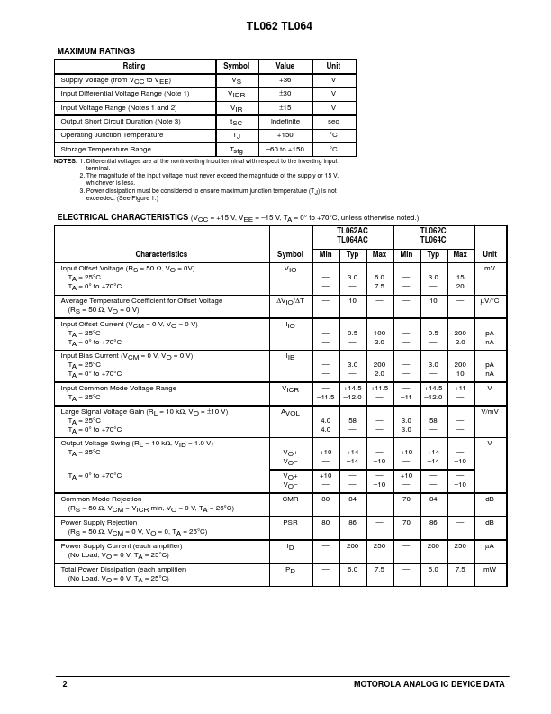
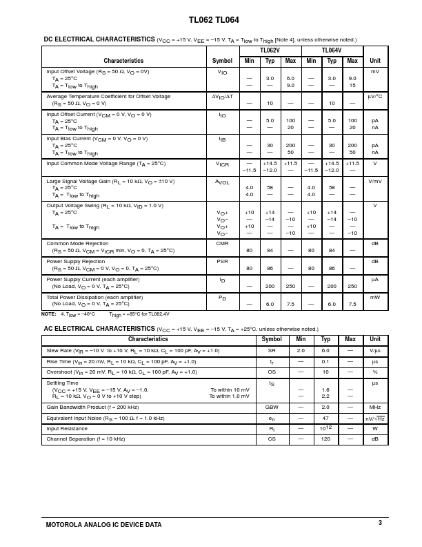
Motorola TL064
LOW POWER JFET INPUT OPERATIONAL AMPLIFIERS
| Part No. | TL064 |
|---|---|
| Datasheet | TL064 Download |
| Manufacturer |  Motorola |
| Description | LOW POWER JFET INPUT OPERATIONAL AMPLIFIERS |
| Buy | Stock & Price |
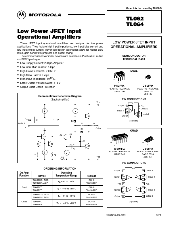
Order this document by TL062/D Low Power JFET Input Operational Amplifiers These JFET input operational amplifiers are designed for low power applications. They feature high input impedance, low input bias current and low input offset current. Advanced design techniques allow for higher slew rates, gain bandwidth products and output swing. The commercial and vehicular devices are available in Plastic dual in–line and SOIC packages.
● Low Supply Current: 200 µA/Amplifier
● Low Input Bias Current: 5.0 pA
● High Gain Bandwidth: 2.0 MHz
● High Slew Rate: 6.0 V/µs
● High Input Impedance: 1012 Ω
● Large Output Voltage Swing: ±14 V
● Output Short Circuit Protection Representative Schematic Diagram (Each Amplifier) VCC Inputs – + J1 J2 + Q3 Q1 Q2 Q4 D2 C1 Q5 Q7 R3 R4 D1 Output C2 Q6 R1 R2 R5 VEE Op Amp Function Dual Quad ORDERING INFORMATION Device Operating Temperature Range TL062CD, ACD TL062CP, ACP TA = 0° to +70°C TL062VD TL062VP TA = –40° to