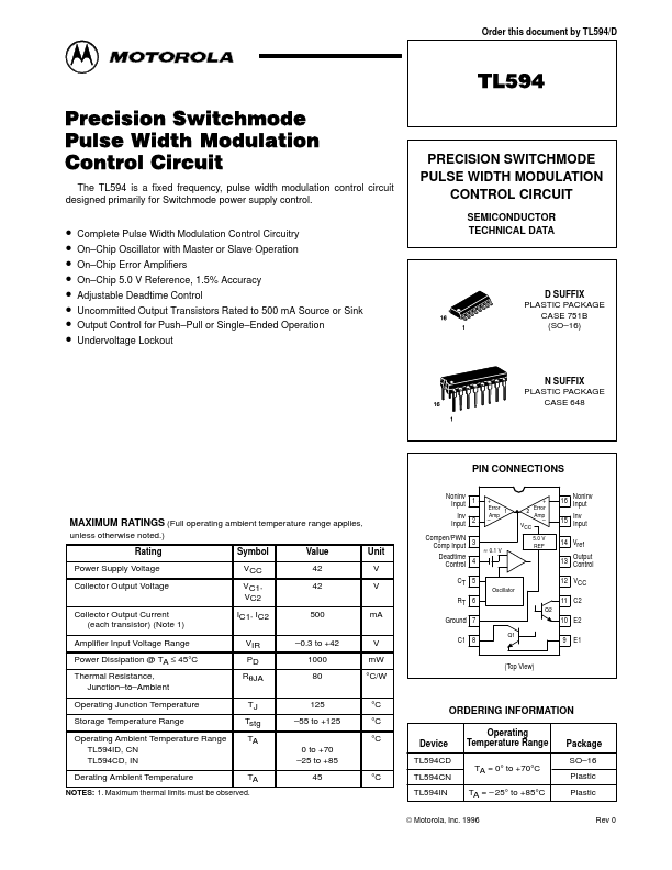
MAXIMUM RATINGS
(Full operating ambient temperature range applies, unless otherwise noted.) Rating Power Supply Voltage Collector Output Voltage Collector Output Current (each transistor) (Note 1) Amplifier Input Voltage Range Power Dissipation @ TA ≤ 45°C Thermal Resistance, Junction–to–Ambient Operating Junction Temperature Storage Temperature Range Operating Ambient Temperature Range TL594ID, CN TL594CD, IN Derating Ambient Temperature Symbol VCC VC1, VC2 IC1, IC2 VIR PD RθJA TJ Tstg TA 0 to +70 –25 to +85 TA 45 °C Value 42 42 500 –0.3 to +42 1000 80 125 –55 to +125 Unit V V mA V mW °C/W °C °C °C Device TL594CD TL594CN TL594IN Inv Input 2 Compen/PWN Comp Input 3 Deadtime Control 4 CT 5 ≈ 0.1 V Oscillator RT 6 Q2 11 C2 10 E2 Q1 Ground 7 C1 8 9 E1 (Top View) ORDERING INFORMATION Operating Temperature Range TA = 0° to +70°C TA = – 25° to +85°C Package SO–16 Plastic Plastic Rev 0 NOTES: 1. Maximum thermal limits must be observed. © Motorola, Inc. 1996 MOTOROLA ANALOG IC DEVICE DATA 1 TL... Motorola