MAXIMUM RATINGS
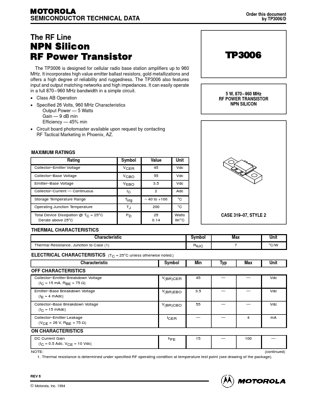
Rating Collector–Emitter Voltage Collector–Base Voltage Emitter–Base Voltage Collector–Current — Continuous Storage Temperature Range Operating Junction Temperature Total Device Dissipation @ TC = 25°C Derate above 25°C Symbol VCER VCBO VEBO IC Tstg TJ PD Value 45 55 3.5 2 – 40 to +100 200 25 0.14 Unit Vdc Vdc Vdc Adc °C °C Watts W/°C CASE 319–07, STYLE 2 THERMAL CHARACTERISTICS Characteristic Thermal Resistance, Junction to Case (1) Symbol RθJC Max 7 Unit °C/W ELECTRICAL CHARACTERISTICS
(TC = 25°C unless otherwise noted.) Characteristic Symbol Min Typ Max Unit OFF CHARACTERISTICS Collector–Emitter Breakdown Voltage (IC = 15 mA, RBE = 75 Ω) Emitter–Base Breakdown Voltage (IE = 4 mAdc) Collector–Base Breakdown Voltage (IC = 15 mAdc) Collector–Emitter Leakage (VCE = 26 V, RBE = 75 Ω) V(BR)CER V(BR)EBO V(BR)CBO ICER 45 3.5 55 — — — — — — — — 4 Vdc Vdc Vdc mA ON CHARACTERISTICS DC Current Gain (IC = 0.5 Adc, VCE = 10 Vdc) hFE 15 — 100 — NOTE: (continued) 1. Thermal resistance is determined under specified RF operating condition at temperature test point (see drawing of the package). Motorola