Motorola VN10LM
TMOS FET Transistor
| Part No. | VN10LM |
|---|---|
| Datasheet | VN10LM Download |
| Manufacturer |  Motorola |
| Description | TMOS FET Transistor |
| Buy | Stock & Price |
MAXIMUM RATINGS
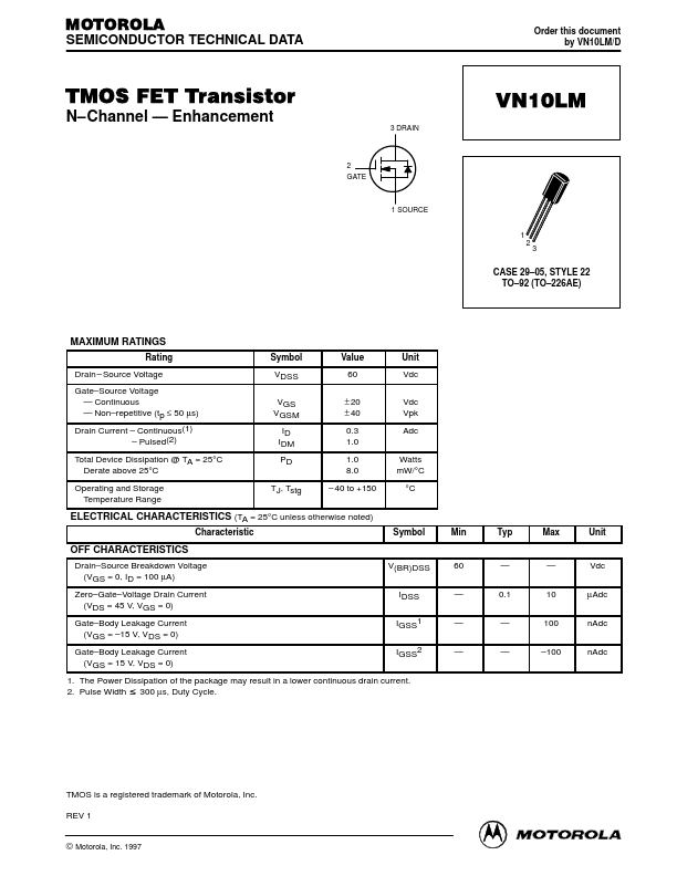
Rating Symbol Value Unit Drain – Source Voltage Gate–Source Voltage — Continuous — Non–repetitive (tp ≤ 50 µs) Drain Current – Continuous(1) – Pulsed(2) Total Device Dissipation @ TA = 25°C Derate above 25°C VDSS VGS VGSM ID IDM PD 60 Vdc ± 20 Vdc ± 40 Vpk 0.3 Adc 1.0 1.0 Watts 8.0 mW/°C Operating and Storage Temperature Range TJ, Tstg – 40 to +150 °CELECTRICAL CHARACTERISTICS
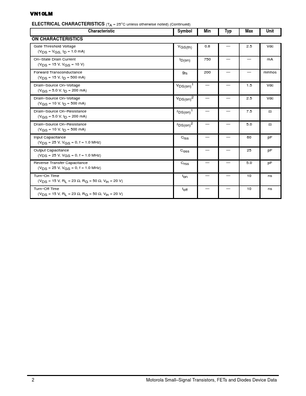
(TA = 25°C unless otherwise noted) Characteristic Symbol OFF CHARACTERISTICS Drain–Source Breakdown Voltage (VGS = 0, ID = 100 µA) Zero–Gate–Voltage Drain Current (VDS = 45 V, VGS = 0) Gate–Body Leakage Current (VGS = –15 V, VDS = 0) Gate–Body Leakage Current (VGS = 15 V, VDS = 0) V(BR)DSS IDSS IGSS1 IGSS2 v1. The Power Dissipation of the package