Datasheet4U.com
🌙
2N6292 Datasheet | Multicomp
Part:
2N6292
Description:
Bipolar Transistor
Category:
Transistor
Manufacturer:
Multicomp
Size:
192.10 KB
2N6292 Datasheet (PDF) Download
Multicomp
2N6292
Overview
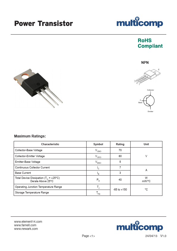
Transistor, NPN, 7A, 70V, TO-220 Part Number 2N6292 Important Notice : This data sheet and its.
Datasheets by Manufacturer
2N6292
— Savantic — Silicon NPN Power Transistors
2N6292
— Central Semiconductor — COMPLEMENTARY SILICON POWER TRANSISTORS
2N6292
— Semelab — HIGH SPEED MEDIUM POWER COMPLEMENTARY PAIR TRANSISTORS
2N6292
— Rectron — Power Transistors
2N6292
— GE — NPN POWER TRANSISTORS
×
Close
This website uses cookies or similar technologies, to enhance your browsing experience and provide personalized recommendations.
By continuing to use our website, you agree to our
Privacy Policy
Accept