ABSOLUTE MAXIMUM RATINGS
(Ta = 25°C) Parameter Collector to base voltage Collector to emitter voltage Emitter to base voltage Collector current Total power dissipation Junction temperature Storage temperature * RBE = 30 kΩ Symbol VCBO VCER * VEBO IC PT Tj Tstg Ratings −80 −80 −5.0 −100 250 125 −55 to +125 Unit V V V mA mW °C °C ELECTRICAL CHARACTERISTICS
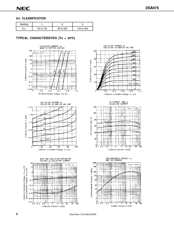
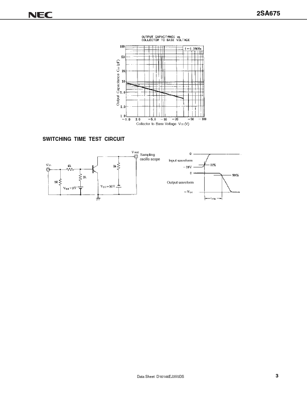
(Ta = 25°C) Parameter Collector cutoff current Emitter cutoff current DC current gain DC current gain Collector saturation voltage Base saturation voltage Gain bandwidth product Output capacitance Storage time Symbol ICBO IEBO hFE1 hFE2 VCE(sat) VBE(sat) fT Cob tstg Conditions VCB = –60 V, IE = 0 VEB = –3.0 V, IC = 0 VCE = –3.0 V, IC = –1.0 mA VCE = –3.0 V, IC = –20 mA IC = –20 mA, IB = –1.0 mA IC = –20 mA, IB = –1.0 mA VCE = –6.0 V, IE = 10 mA VCB = –10 V, IE = 0, f = 1.0 MHz Refer to the test circuit. PACKAGE DRAWING (UNIT: mm) MIN. 60 50 100 TYP. 120 120 −0.10 −0.74 170 4.5 0.5 MAX. −1.0 −1.0 300 −1.50 −1.20 10 1.0 Unit µA µA V V MHz pF µs The information in this document is subject to change without notice. NEC