DESCRIPTION
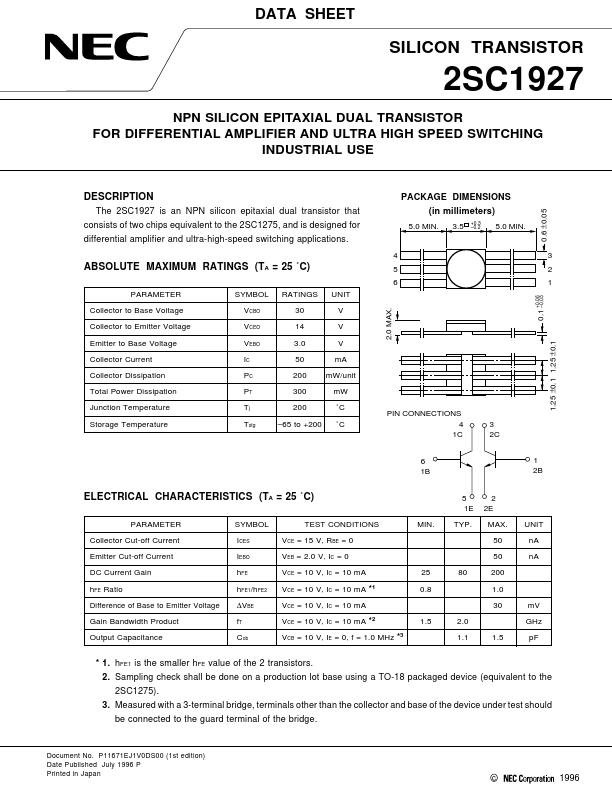
4 PACKAGE DIMENSIONS 5.0 MIN. 3.5 +0.3 –0.2 5.0 MIN. ABSOLUTE MAXIMUM RATINGS
(TA = 25 ˚C) PARAMETER Collector to Base Voltage Collector to Emitter Voltage Emitter to Base Voltage Collector Current Collector Dissipation Total Power Dissipation Junction Temperature Storage Temperature SYMBOL VCBO VCEO VEBO IC PC PT Tj Tstg RATINGS 30 14 3.0 50 200 300 200 –65 to +200 UNIT 2.0 MAX. 5 6 0.1 +0.06 –0.03 V V V mA mW/unit mW ˚C ˚C PIN CONNECTIONS 4 1C 6 1B 3 2C 1 2B ELECTRICAL CHARACTERISTICS
(TA = 25 ˚C) PARAMETER Collector Cut-off Current Emitter Cut-off Current DC Current Gain hFE Ratio Difference of Base to Emitter Voltage Gain Bandwidth Product Output Capacitance SYMBOL ICES IEBO hFE hFE1/hFE2 ∆VBE fT Cob TEST CONDITIONS VCE = 15 V, RBE = 0 VEB = 2.0 V, IC = 0 VCE = 10 V, IC = 10 mA VCE = 10 V, IC = 10 mA *1 VCE = 10 V, IC = 10 mA VCE = 10 V, IC = 10 mA *2 *3 1.5 25 0.8 MIN. 5 1E TYP. 2 2E MAX. 50 50 UNIT nA nA 80 200 1.0 30 mV GHz 1.5 pF 2.0 1.1 VCB = 10 V, IE = 0, f = 1.0 MHz * 1. hFE1 is the smaller hFE value of the 2 transistors. NEC