2SK2479
2SK2479 is N-Channel MOSFET manufactured by NEC.
DESCRIPTION
The 2SK2479 is N-Channel MOS Field Effect Transistor designed for high voltage switching applications.
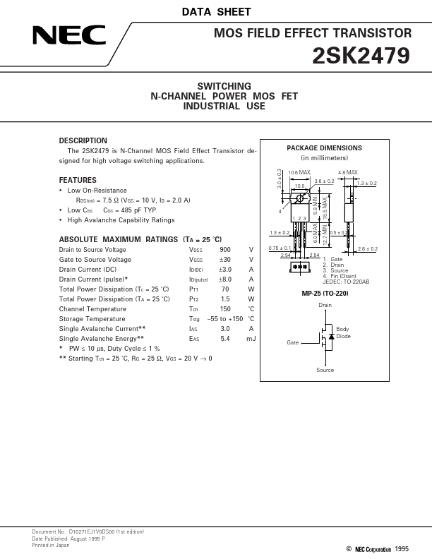
3.0 ± 0.3
PACKAGE DIMENSIONS (in millimeters)
10.6 MAX. 3.6 ± 0.2 10.0 5.9 MIN. 12.7 MIN. 15.5 MAX. 4.8 MAX. 1.3 ± 0.2
FEATURES
- Low On-Resistance
RDS(on) = 7.5 Ω (VGS = 10 V, ID = 2.0 A)
6.0 MAX.
- Low Ciss Ciss = 485 p F TYP.
- High Avalanche Capability Ratings
ABSOLUTE MAXIMUM RATINGS (TA = 25 ˚C)
Drain to Source Voltage Gate to Source Voltage Drain Current (DC) Drain Current (pulse)- Total Power Dissipation (Tc = 25 ˚C) Total Power Dissipation (TA = 25 ˚C) Channel Temperature Storage Temperature Single Avalanche Current-
- Single Avalanche Energy-
- - PW ≤ 10 µs, Duty Cycle ≤ 1 % VDSS VGSS ID(DC) ID(pulse) PT1 PT2 Tch Tstg IAS EAS 900 ± 30 ± 3.0 ± 8.0 70 1.5 150 3.0 5.4 V V A A W W ˚C A m J
4 1 2 3 1.3 ± 0.2 0.75 ± 0.1 2.54
0.5 ± 0.2 2.8 ± 0.2
1. Gate 2. Drain 3. Source 4. Fin (Drain) JEDEC: TO-220AB
MP-25 (TO-220)
Drain
- 55 to +150 ˚C
Body Diode Gate
- - Starting Tch = 25 ˚C, RG = 25 Ω, VGS = 20 V → 0
Source
Document No. D10271EJ1V0DS00 (1st edition) Date Published August 1995 P Printed in Japan
©
ELECTRICAL CHARACTERISTICS (TA = 25 ˚C)
CHARACTERISTIC Drain to Source On-State Resistance Gate to Source Cutoff Voltage Forward Transfer Admittance Drain Leakage Current Gate to Source Leakage Current Input Capacitance Output Capacitance Reverse Transfer Capacitance Turn-On Delay Time Rise Time Turn-Off Delay Time Fall Time Total Gate Charge Gate to Source Charge Gate to Drain Charge Body Diode Forward Voltage Reverse Recovery Time Reverse Recovery Charge SYMBOL RDS(on) VGS(off) | yfs | IDSS IGSS Ciss Coss Crss td(on) tr td(off) tf QG QGS QGD VF(S-D) trr Qrr 485 75 10 12 5 35 8 17 3 8 1.0 670 3.0 2.5 0.8 100 ± 100 MIN. TYP. 5.6 MAX. 7.5 3.5 UNIT Ω V S TEST CONDITIONS VGS = 10 V, ID = 2.0 A VDS = 10 V, ID = 1 m A VDS = 20 V, ID = 2.0 A VDS = VDSS, VGS = 0 VGS = ± 30 V, VDS = 0 VDS = 10 V VGS = 0 f = 1 MHz ID = 2.0 A VGS = 10...