2SK2597
FEATURES
- High output, high gain PO = 100 W, GL = 13 d B (TYP.) (f = 900 MHz) PO = 90 W, GL = 12 d B (TYP.) (f = 960 MHz)
- Low intermodulation distortion
- Covers all base station frequencies such as 800-MHz PDC and GSM
- High-reliability gold electrodes
- Hermetic sealed package
- Internal matching circuit
- Push-pull structure
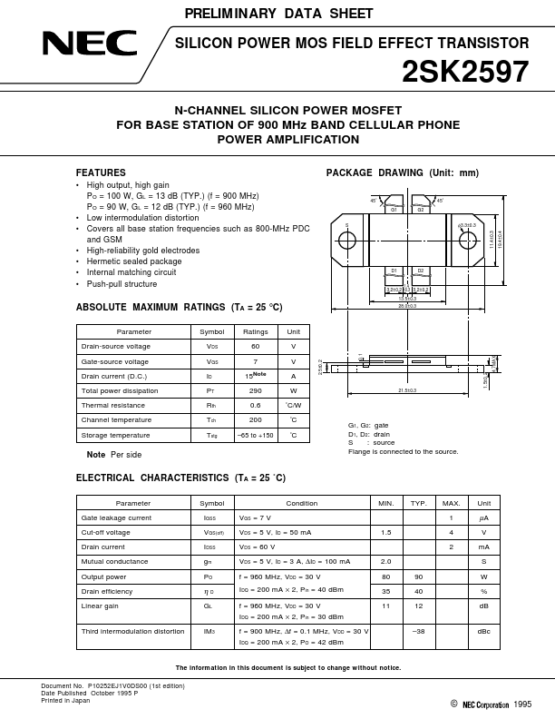
PACKAGE DRAWING (Unit: mm)
45˚ G1 S G2 45˚
φ 3.3±0.3
11.4±0.3 19.4±0.4
D1
D2
1.4 3.2±0.2 ±0.3 3.2±0.2 13.5±0.3 28.0±0.3
ABSOLUTE MAXIMUM RATINGS (TA = 25 °C)
Parameter Drain-source voltage Gate-source voltage Drain current (D.C.) Total power dissipation Thermal resistance Channel temperature Storage temperature Symbol VDS VGS ID PT Rth Tch Tstg Ratings 60 7 15Note 290 0.6 200
- 65 to +150 Unit V
0.1 2.5±0.2
V A W ˚C/W ˚C ˚C
21.5±0.3
Note Per side
G1, G2: gate D1, D2: drain S : source Flange is connected to the source.
ELECTRICAL CHARACTERISTICS (TA = 25 ˚C)
Parameter Gate leakage current Cut-off voltage Drain current Mutual conductance Output power...