2SK3663
2SK3663 is N-CHANNEL MOS FIELD EFFECT TRANSISTOR manufactured by NEC.
DESCRIPTION
The 2SK3663 is a switching device which can be driven directly by a 2.5 V power source. .. The 2SK3663 features a low on-state resistance and excellent switching characteristics, and is suitable for applications such as power switch of portable machine and so on.
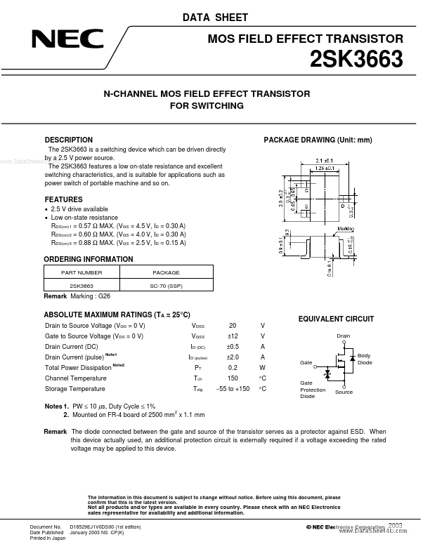
PACKAGE DRAWING (Unit: mm)
FEATURES
- 2.5 V drive available
- Low on-state resistance RDS(on)1 = 0.57 Ω MAX. (VGS = 4.5 V, ID = 0.30 A) RDS(on)2 = 0.60 Ω MAX. (VGS = 4.0 V, ID = 0.30 A) RDS(on)3 = 0.88 Ω MAX. (VGS = 2.5 V, ID = 0.15 A)
ORDERING INFORMATION
PART NUMBER 2SK3663 PACKAGE SC-70 (SSP)
Remark Marking : G26
ABSOLUTE MAXIMUM RATINGS (TA = 25°C)
Drain to Source Voltage (VGS = 0 V) Gate to Source Voltage (VDS = 0 V) Drain Current (DC) Drain Current (pulse)
Note1 Note2
EQUIVALENT CIRCUIT
VDSS VGSS ID (DC) 20 ±12 ±0.5 ±2.0 0.2 150
- 55 to +150 V V A A W °C °C
Gate Body Diode Drain
ID (pulse) PT Tch Tstg
Total Power Dissipation Channel Temperature Storage Temperature
Gate Protection Diode
Source
Notes 1. PW ≤ 10 µs, Duty Cycle ≤ 1% 2 2. Mounted on FR-4 board of 2500 mm x 1.1 mm Remark The diode connected between the gate and source of the transistor serves as a protector against ESD. When this device actually used, an additional protection circuit is externally required if a voltage exceeding the rated voltage may be applied to this device.
The information in this document is subject to change without notice. Before using this document, please confirm that this is the latest version.
Not all products and/or types are available in every country. Please check with an NEC Electronics sales representative for availability and additional information.
Document No. D16529EJ1V0DS00 (1st edition) Date Published January 2003 NS CP(K) Printed in Japan
ELECTRICAL CHARACTERISTICS (TA = 25°C)
CHARACTERISTICS Zero Gate Voltage Drain Current Gate Leakage Current Gate Cut-off Voltage
Note
SYMBOL IDSS IGSS VGS(off) | yfs |
Note
TEST CONDITIONS VDS = 20 V, VGS = 0 V VGS = ±12 V,...