2SK4143
2SK4143 is SWITCHING N-CHANNEL POWER MOSFET manufactured by NEC.
DESCRIPTION
The 2SK4143 is N-channel MOS Field Effect Transistor designed for high current switching applications.
FEATURES
- Low on-state resistance RDS(on)1 = 44 mΩ MAX. (VGS = 10 V, ID = 10 A) RDS(on)2 = 78 mΩ MAX. (VGS = 4.0 V, ID = 10 A)
- Low input capacitance Ciss = 820 p F TYP.
- Built-in gate protection diode
ORDERING INFORMATION
PART NUMBER 2SK4143-S17-AY
Note
LEAD PLATING Pure Sn (Tin)
PACKING Tube 50 p/tube
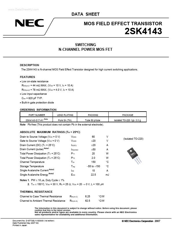
PACKAGE Isolated TO-220 typ. 2.2 g
Note Pb-free (This product does not contain Pb in the external electrode).
ABSOLUTE MAXIMUM RATINGS (TA = 25°C)
Drain to Source Voltage (VGS = 0 V) Gate to Source Voltage (VDS = 0 V) Drain Current (DC) (TC = 25°C) Drain Current (pulse)
Note1
VDSS VGSS ID(DC) ID(pulse) PT1 PT2 Tch Tstg
60 ±20 ±20 ±50 20 2.0 150
- 55 to +150 15 22.5
V V A A W W °C °C A m J
(Isolated TO-220)
Total Power Dissipation (TC = 25°C) Total Power Dissipation (TA = 25°C) Channel Temperature Storage Temperature Single Avalanche Current Single Avalanche Energy
Note2 Note2
IAS EAS
Notes 1. PW ≤ 10 μs, Duty Cycle ≤ 1% 2. Tch ≤ 150°C, VDD = 30 V, RG = 25 Ω, VGS = 20 → 0 V, L = 100 μH
THERMAL RESISTANCE
Channel to Case Thermal Resistance Channel to Ambient Thermal Resistance Rth(ch-C) Rth(ch-A) 6.25 62.5 °C/W °C/W
The information in this document is subject to change without notice. Before using this document, please confirm that this is the latest version.
Not all products and/or types are available in every country. Please check with an NEC Electronics sales representative for availability and additional information.
Document No. D18772EJ1V0DS00 (1st edition) Date Published May 2007 NS Printed in Japan
ELECTRICAL CHARACTERISTICS (TA = 25°C)
CHARACTERISTICS Zero Gate Voltage Drain Current Gate Leakage Current Gate to Source Cut-off Voltage Forward Transfer Admittance
Note Note
SYMBOL IDSS IGSS VGS(off) | yfs | RDS(on)1 RDS(on)2
TEST CONDITIONS VDS = 60 V, VGS = 0 V VGS = ±20 V, VDS = 0 V VDS = 10 V, ID = 1 m A VDS = 10...