K2723
DESCRIPTION
This product is N-Channel MOS Field Effect Transistor designed for high current switching spplications. ..
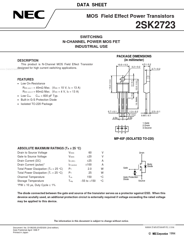
15.0 ± 0.3
3 ± 0.1 4 ± 0.2
- Low On-Resistance RDS (on) 1 = 40mΩ Max. (VGS = 10 V, ID = 13 A) RDS (on) 2 = 60mΩ Max. (VGS = 4 V, ID = 13 A) Ciss = 830 p F Typ.
- Low Ciss
- Built-in G-S Protection Diode
- Isolated TO-220 Package
0.7 ± 0.1 2.54
1.3 ± 0.2 1.5 ± 0.2 2.54
13.5MIN.
12.0 ± 0.2
FEATURES
2.5 ± 0.1 0.65 ± 0.1 1.Gate 2.Drain 3.Source
1 2 3
MP-45F (ISOLATED TO-220)
ABSOLUTE MAXIMUM RATINGS (TA = 25 °C)
Drain to Source Voltage Gate to Source Voltage Drain Current (DC) Drain Current (pulse)- Total Power Dissipation (TA = 25 °C) Total Power Dissipation (Tc = 25 °C) Channel Temperature Storage Temperature
- PW ≤ 10 µs, Duty Cycle ≤ 1% The diode connected between the gate and source of the transistor serves as a protector against ESD. When this deveice acutally used, an addtional protection circiut is externally required if voltage exceeding the rated...