NEC UPD70F3711
32-Bit Single-Chip Microcontrollers
| Part No. | UPD70F3711 |
|---|---|
| Datasheet | UPD70F3711 Download |
| Manufacturer |  NEC |
| Description | 32-Bit Single-Chip Microcontrollers |
| Buy | Stock & Price |
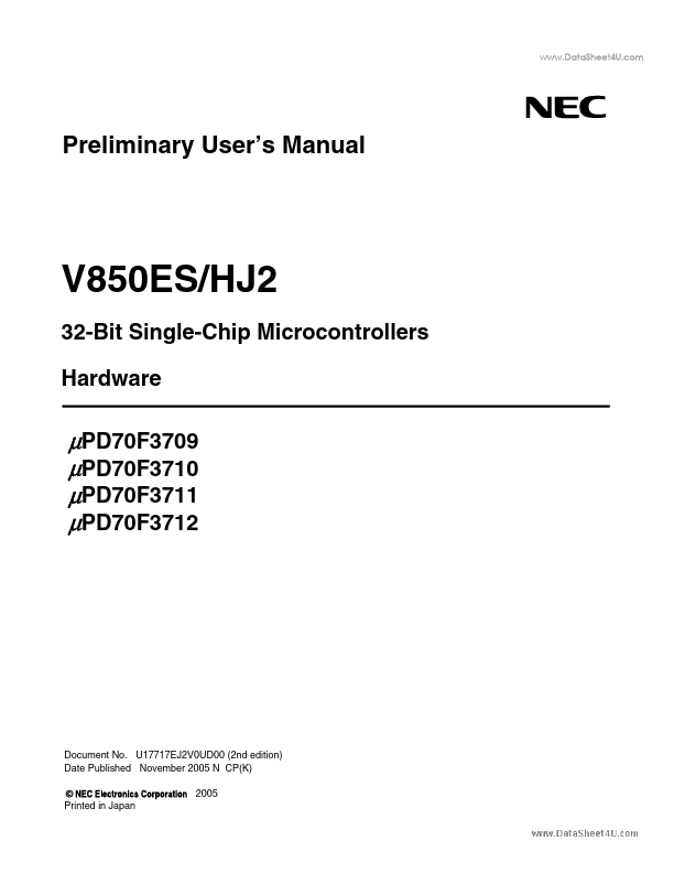
Preliminary User’s Manual V850ES/HJ2 32-Bit Single-Chip Microcontrollers Hardware µPD70F3709 µPD70F3710 µPD70F3711 µPD70F3712 Document No. U17717EJ2V0UD00 (2nd edition) Date Published November 2005 N CP(K) 2005 Printed in Japan [MEMO] 2 Preliminary User’s Manual U17717EJ2V0UD NOTES FOR CMOS DEVICES 1 VOLTAGE APPLICATION WAVEFORM AT INPUT PIN Waveform distortion due to input noise or a reflected wave may cause malfunction. If the input of the CMOS device stays in the area between VIL (MAX) and VIH (MIN) due to noise, etc., the device may malfunction. Take care to prevent chattering noise from entering the device when the input level is fixed, and also in the transition period when the input level passes through the area between VIL (MAX) and VIH (MIN). 2 HANDLING OF UNUSED INPUT PINS Unconnected CMOS device inputs can be cause of malfunction. If an input pin is unconnected, it is possible that an internal input level may be generated due to noise, etc., causing malfunction. CMOS devices behave differently than Bipolar or NMOS devices.