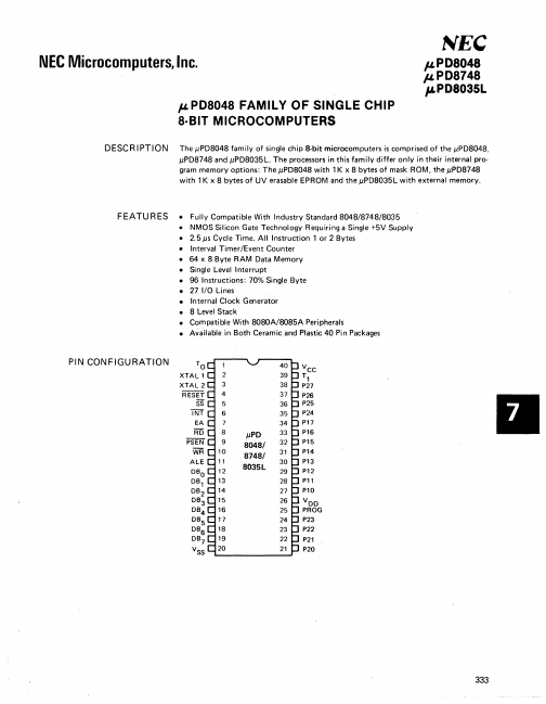
DESCRIPTION
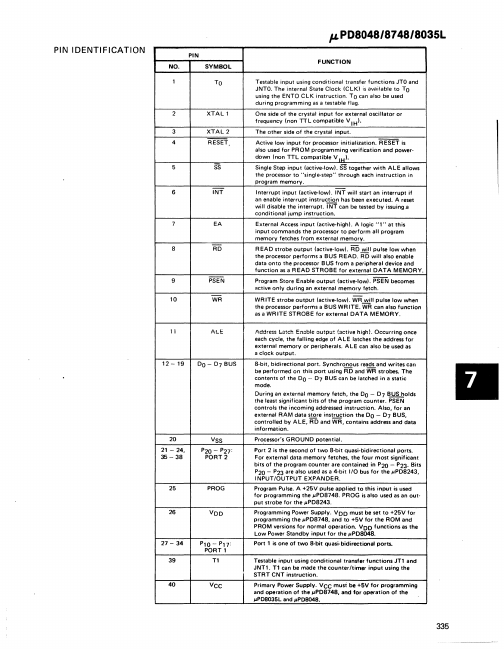
BLOCK DIAGRAM 334 "cC'''UST IV,",fU",BU WOAO LEfIrIGTHI PIN IDENTIFICATION PIN NO. SYMBOL 1 TO 2 XTALI 3 XTAL2 4 RESET 5 SS 6 INT 7 EA 8 RD 9 PSEN 10 WR 11 ALE 12 - 19 DO - D7 BUS 20 21- 24, 35-38 VSS P20 - P27: PORT 2 25 PROG 26 VDD 27 - 34 39 Pl0 - P17: PORT 1 T1 40 Vce fL PD8048/8748/8035L FUNCTION Testable input using conditional transfer functions JTO and JNTO. TO can also be used during programming as a testable flag. One side of the crystal input for external oscillator or Irequency (non TIL compatible V IH). The other side of the crystal input. Active low input for processor initialization. RESET is also used for PROM programming verification and powerdown (non TTL compatible V~. Single Step input (active●low). SS together with ALE allows the processor to "single-step" through each instruction in program memory. Interrupt input (active-low). tNT will start an interrupt if an enable interrupt instruction has been executed. A reset will disable the interrupt. INT can be t.sted by issuing a conditional jump instruction. NEC