Datasheet4U Logo Datasheet4U.com

UPG175TA - L-Band PA DRIVER AMPLIFIER

Datasheet Summary

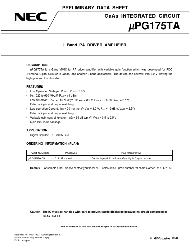
Description

(Personal Digital Cellular in Japan) and another L-band application.

The device can operate with 3.0 V, having the high gain and low distortion.

Features

  • Low Operation Voltage: VDD1 = VDD2 = 3.0 V.
  • fRF: 925 to 960 MHz@ Pout = +9 dBm.
  • Low distortion: Padj1 =.
  • 60 dBc typ. @ VDD = 3.0 V, Pout = +9 dBm, VAGC = 2.5 V External input and output matching.
  • Low operation Current: IDD = 20 mA typ. @ VDD = 3.0 V, Pout = +9 dBm, VAGC = 2.5 V External input and output matching.
  • Variable gain control function: ∆G = 35 dB typ. @ VAGC = 0.5 to 2.5 V.
  • 6 pin mini-mold package.

📥 Download Datasheet

Datasheet preview – UPG175TA

Datasheet Details

Part number UPG175TA
Manufacturer NEC
File Size 62.02 KB
Description L-Band PA DRIVER AMPLIFIER
Datasheet download datasheet UPG175TA Datasheet
Additional preview pages of the UPG175TA datasheet.
Other Datasheets by NEC

Full PDF Text Transcription

Click to expand full text
PRELIMINARY DATA SHEET GaAs INTEGRATED CIRCUIT µPG175TA L-Band PA DRIVER AMPLIFIER DESCRIPTION µPG175TA is a GaAs MMIC for PA driver amplifier with variable gain function which was developed for PDC (Personal Digital Cellular in Japan) and another L-band application. The device can operate with 3.0 V, having the high gain and low distortion. FEATURES • Low Operation Voltage: VDD1 = VDD2 = 3.0 V • fRF: 925 to 960 MHz@ Pout = +9 dBm • Low distortion: Padj1 = –60 dBc typ. @ VDD = 3.0 V, Pout = +9 dBm, VAGC = 2.5 V External input and output matching • Low operation Current: IDD = 20 mA typ. @ VDD = 3.0 V, Pout = +9 dBm, VAGC = 2.5 V External input and output matching • Variable gain control function: ∆G = 35 dB typ. @ VAGC = 0.5 to 2.
Published: |