NETSOL S7S3218T4M
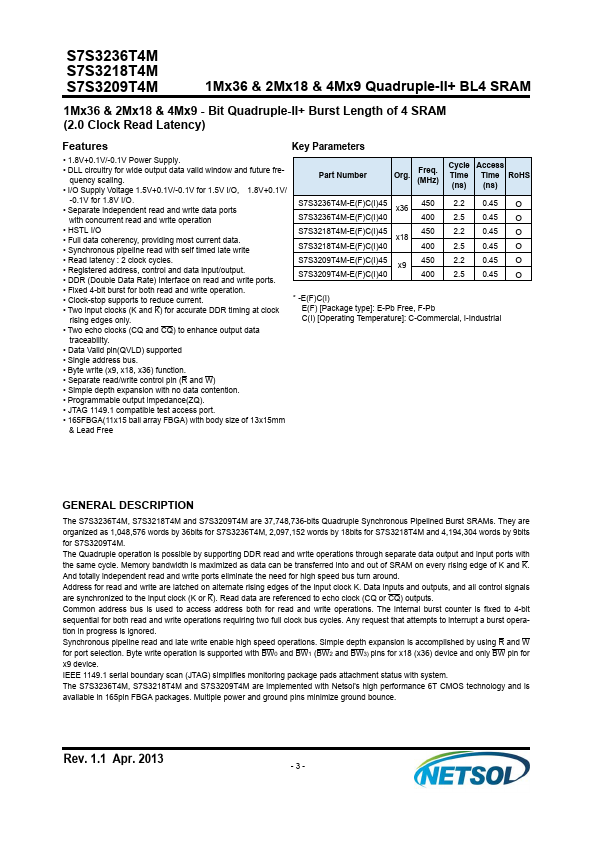
The S7S3236T4M, S7S3218T4M and S7S3209T4M are 37,748,736-bits Quadruple Synchronous Pipelined Burst SRAMs. They are organized as 1,048,576 words by 36bits for S7S3236T4M, 2,097,152 words by 18bits for S7S3218T4M and 4,194,304 words by 9bits for S7S3209T4M. The Quadruple operation is possible by supporting DDR read and write operations through separate data output and input ports with the same cycle.| Part No. | S7S3218T4M |
|---|---|
| Datasheet | S7S3218T4M Download |
| Manufacturer | NETSOL |
| Description | 1Mx36 & 2Mx18 & 4Mx9 Quadruple-II+ BL4 SRAM |
| Buy | Stock & Price |
FEATURES
KEY PARAMETERS
●1.8V+0.1V/-0.1V Power Supply.●DLL circuitry for wide output data valid window and future fre- quency scaling.
● I/O Supply Voltage 1.5V+0.1V/-0.1V for 1.5V I/O, 1.8V+0.1V/ Part Number Org. Freq. (MHz) Cycle Access Time Time RoHS (ns) (ns) -0.1V for 1.8V I/O
●Separate independent read and write data ports with concurrent read and write operation S7S3236T4M-E(F)C(I)45 x36 450 2.2 0.45 S7S3236T4M-E(F)C(I)40 400 2.5 0.45
● HSTL I/O
● Full data coherency, providing most current data.
● Synchronous pipeline read with self timed late write S7S3218T4M-E(F)C(I)45 x18 450 2.2 0.45 S7S3218T4M-E(F)C(I)40 400 2.5 0.45
● Read latency : 2 clock cycles.
● Registered address, control and data input/output.
● DDR (Double Data Rate) Interface on read and write ports. S7S3209T4M-E(F)C(I)45 x9 450 2.2 0.45 S7S3209T4M-E(F)C(I)40 400 2.5 0.45
● Fixed 4-bit burst for both read and write operation.
● Clock-stop supports to reduce current.
●Two input clocks (K and K) f...