P1306EK
P1306EK is P-Channel Enhancement Mode Field Effect Transistor manufactured by NIKO-SEM.
- Part of the P1306EK-NIKO comparator family.
- Part of the P1306EK-NIKO comparator family.
NIKO-SEM
P-Channel Logic Level Enhancement Mode P1306EK
Field Effect Transistor
PDFN 5x6P
Halogen-Free & Lead-Free
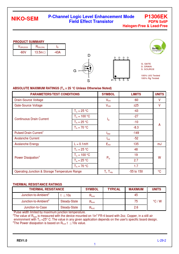
PRODUCT SUMMARY
V(BR)DSS
RDS(ON)
-60V
13.5mΩ
ID -43A
D DDD #1 S S S G
G. GATE D. DRAIN S. SOURCE
100% UIS Tested 100% Rg Tested
ABSOLUTE MAXIMUM RATINGS (TA = 25 °C Unless Otherwise Noted)
PARAMETERS/TEST CONDITIONS
SYMBOL
Drain-Source Voltage
Gate-Source Voltage
TC = 25 °C
Continuous Drain Current
TC = 100 °C TA = 25 °C
Pulsed Drain Current1
TA = 70 °C
Avalanche Current
Avalanche Energy
L = 0.1m H
TC = 25 °C
Power Dissipation3
TC = 100 °C TA = 25 °C
TA = 70 °C
Operating Junction & Storage Temperature Range
VDS VGS
IDM IAS EAS
Tj, Tstg
LIMITS -60 ±25 -43 -27 -10 -8.3 -149 -52 135 48 19 2.7 1.7
-55 to...