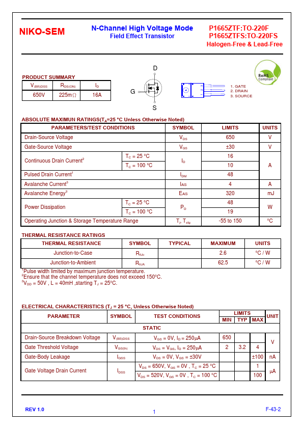
Download the P1665ZTFS datasheet PDF.
This datasheet also covers the P1665ZTF-NIKO variant, as both devices belong to the same n-channel mosfet family and are provided as variant models within a single manufacturer datasheet.
Full PDF Text Transcription for P1665ZTFS (Reference)
Note: Below is a high-fidelity text extraction (approx. 800 characters) for
P1665ZTFS. For precise diagrams, and layout, please refer to the original PDF.
NIKO-SEM N-Channel High Voltage Mode Field Effect Transistor P1665ZTF:TO-220F P1665ZTFS:TO-220FS Halogen-Free & Lead-Free PRODUCT SUMMARY V(BR)DSS RDS(ON) 650V 225mΩ ID 1...
View more extracted text
ogen-Free & Lead-Free PRODUCT SUMMARY V(BR)DSS RDS(ON) 650V 225mΩ ID 16A D G S ABSOLUTE MAXIMUN RATINGS(TA=25 °C Unless Otherwise Noted) PARAMETERS/TEST CONDITIONS SYMBOL Drain-Source Voltage Gate-Source Voltage Continuous Drain Current2 Pulsed Drain Current1 Avalanche Current3 Avalanche Energy3 TC = 25 °C TC = 100 °C Power Dissipation TC = 25 °C TC = 100 °C Operating Junction & Storage Temperature Range VDS VGS ID IDM IAS EAS PD Tj, Tstg THERMAL RESISTANCE RATINGS THERMAL RESISTANCE SYMBOL TYPICAL Junction-to-Case RJc Junction-to-Ambient RJA 1Pulse width limited by maximum junction temperature. 2Ensure that the channel