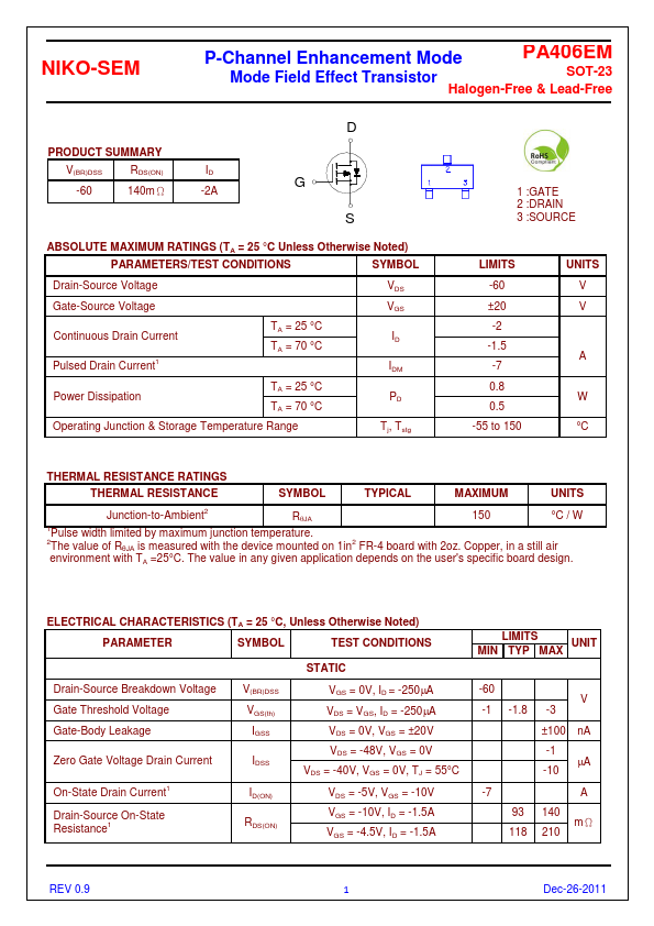
PA406EM
NIKO-SEM
P-Channel Enhancement Mode
Mode Field Effect Transistor
SOT-23
Halogen-Free & Lead-Free
PRODUCT SUMMARY
V(BR)DSS
RDS(ON)
-60 140mΩ
ID -2A
ABSOLUTE MAXIMUM RATINGS (TA = 25 °C Unless Otherwise Noted)
PARAMETERS/TEST CONDITIONS
SYMBOL
Drain-Source Voltage
Gate-Source Voltage
Continuous Drain Current Pulsed Drain Current1
TA = 25 °C TA = 70 °C
Power Dissipation
TA = 25 °C TA = 70 °C
Operating Junction & Storage Temperature Range
VDS VGS ID IDM PD Tj, Tstg
1 :GATE 2 :DRAIN 3 :SOURCE
LIMITS -60 ±20 -2 -1.5 -7 0.8 0.5
-55 to 150
UNITS V V
W °C
THERMAL RESISTANCE RATINGS
THERMAL RESISTANCE
SYMBOL
TYPICAL
MAXIMUM
UNITS
Junction-to-Ambient2
RθJA
150 °C / W
1Pulse width limited by maximum junction temperature. 2The value of RθJA is measured with the device mounted on 1in2 FR-4 board with 2oz. Copper, in a still air environment with TA =25°C. The value in any given application depends on the user's specific board...