PV563BA Overview
Key Features
- 40 -1.3 -1.5 -3 V
| Part | PV563BA |
|---|---|
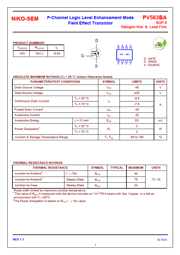
| Description | P-Channel Enhancement Mode Field Effect Transistor |
| Category | Transistor |
| Manufacturer | NIKO-SEM |
| Size | 230.30 KB |
| Part Number | Manufacturer | Description |
|---|---|---|
| PV563BA | UNIKC | P-Channel MOSFET |