BUZ54
BUZ54 is Power MOS Transistor manufactured by NJS.
DESCRIPTION
N-channel enhancement mode field-effect power transistor in a metal envelope. This device is intended for use in Switched Mode Power Supplies (SMPS), motor control, welding, DC/DC and DC/AC converters, and in general purpose switching applications. QUICK REFERENCE DATA SYMBOL PARAMETER Drain-source voltage Drain current (d.c.) Total power dissipation Drain-source on-state resistance
VDS ID ptot
RDS(ON)
MAX. 1000 5,1 125 2,0
UNIT
V A W n
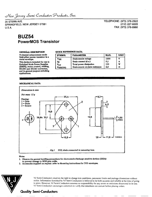
MECHANICAL DATA Dimensions in mm Net mass: 12 g Pinning: 1
- Gate 2 » Drain 3 " Source
25,4
~8,3~
4,2
38,84 30,1
19,5
,^J 1,55 1 max
10,9--
7Z»3««!.3
Ftg. 1
T03; drain connected to mounting base.
Notes 1. Observe the general handling precautions for electrostatic-discharge sensitive devices (ESDs) to prevent damage to MOS gate oxide. 2. Accessories supplied on request: refer to Mounting instructions for TO3 envelopes.
NJ Semi-Conductors reserves the right to change test conditions, parameter limits and package dimensions without notice. Information furnished by NJ Semi-Conductors is believed to.b'eboth accurate and reliable at the time of going to press. However, NJ Semi-Conductors assumes no responsibility for any errors or omissions discovered in its use. NJ Semi-Conductors encourages customers to verify that datasheets are current before placing orders.
Quality Semi-Conductors
RATINGS
Limiting values in accordance with the Absolute Maximum System (IEC 134) M1N. CONDITIONS SYMBOL PARAMETER _ Drain-source voltage VDS Drain-gate voltage RGS = 20 kn VDGR Gate-source voltage ±VGS Drain current (d.c.) T mb
- 25 °C ID Drain current (d.c.) Tmb»100°C ID Drain current (pulse peak value) Tmb= 25 °C !DM Total power dissipation T mb 25 °C Ptot -55 Storage temperature Tstg Junction temperature
- T
- J
MAX. 1000 1000 20 5,1 3,2 20 125 ISO 150
UNIT V
V A A A W °C
°c
THERMAL RESISTANCES
From junction to mounting base From junction to ambient
STATIC CHARACTERISTICS
Rthj-mb-l,OK/W Rthj-a =35 K/W
Tmb
- 25...