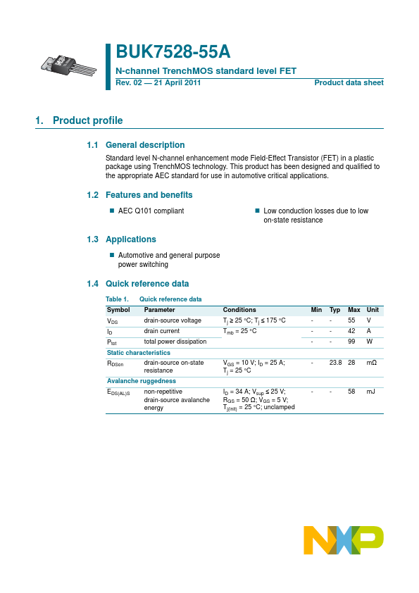
BUK7628-55A
BUK7628-55A is N-Channel MOSFET manufactured by NXP Semiconductors.
- Part of the BUK7528-55A comparator family.
- Part of the BUK7528-55A comparator family.
Philips Semiconductors
Product specification
Trench MOS transistor Standard level FET
GENERAL DESCRIPTION
N-channel enhancement mode standard level field-effect power transistor in a plastic envelope available in TO220AB and SOT404 . Using ’trench’ technology which Features very low on-state resistance. It is intended for use in automotive and general purpose switching applications.
BUK7528-55A BUK7628-55A
QUICK REFERENCE DATA
SYMBOL VDS ID Ptot Tj RDS(ON) PARAMETER Drain-source voltage Drain current (DC) Total power dissipation Junction temperature Drain-source on-state resistance VGS = 10 V MAX. 55 41 99 175 28 UNIT V A W ˚C mΩ
PINNING TO220AB & SOT404
PIN 1 2 3 DESCRIPTION gate drain
2 mb tab
PIN CONFIGURATION
SYMBOL d g
3 SOT404 BUK7628-55A source
1 tab/mb drain
1 2 3 TO220AB BUK7528-55A s
LIMITING VALUES
Limiting values in accordance with the Absolute Maximum System (IEC 134) SYMBOL VDS VDGR ±VGS ID ID IDM Ptot Tstg, Tj PARAMETER Drain-source voltage Drain-gate voltage Gate-source voltage Drain current (DC) Drain current (DC) Drain current (pulse peak value) Total power dissipation Storage & operating temperature CONDITIONS RGS = 20 kΩ Tmb = 25 ˚C Tmb = 100 ˚C Tmb = 25 ˚C Tmb = 25 ˚C MIN.
- 55 MAX. 55 55 20 42 30 168 99 175 UNIT V V V A A A W ˚C
THERMAL RESISTANCES
SYMBOL Rth j-mb Rth j-a Rth j-a PARAMETER Thermal resistance junction to mounting base Thermal resistance junction to ambient(TO220AB) Thermal resistance junction to ambient(SOT404) CONDITIONS in free air Minimum footprint, FR4 board TYP. 60 50 MAX. 1.5 UNIT K/W K/W K/W
June 2000
Rev 1.100
Philips Semiconductors
Product specification
Trench MOS transistor Standard level FET
STATIC CHARACTERISTICS
Tj= 25˚C unless otherwise specified SYMBOL V(BR)DSS VGS(TO) IDSS IGSS RDS(ON) PARAMETER Drain-source breakdown voltage Gate threshold voltage Zero gate voltage drain current Gate source leakage current Drain-source on-state resistance CONDITIONS VGS = 0 V; ID = 0.25 m A; Tj = -55˚C VDS...