PSMN020-30MLC
Overview
Logic level enhancement mode N-channel MOSFET in LFPAK33 package. This product is designed and qualified for use in a wide range of industrial, communications and domestic equipment.
- Low parasitic inductance and resistance
- Optimised for 4.5V Gate drive utilising Superjunction technology
- Ultra low QG, QGD, and QOSS for high system efficiencies at low and high loads 1.3 Applications
- DC-to-DC converters
- Load switching
- Synchronous buck regulator 1.4 Quick reference data Table
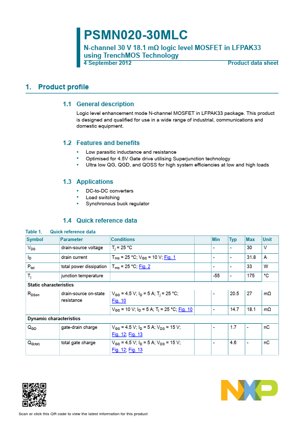
- Symbol VDS ID Ptot Tj RDSon Quick reference data Parameter drain-source voltage drain current total power dissipation junction temperature Conditions Tj = 25 °C Tmb = 25 °C; VGS = 10 V; Fig. 1 Tmb = 25 °C; Fig. 2 Min -55 Typ Max 30 31.8 33 175 Unit V A W °C Static characteristics drain-source on-state resistance VGS = 4.5 V; ID = 5 A; Tj = 25 °C; Fig. 10 VGS = 10 V; ID = 5 A; Tj = 25 °C; Fig. 10 Dynamic characteristics QGD QG(tot) gate-drain charge total gate charge VGS = 4.5 V; ID = 5 A; VDS = 15 V; Fig. 12; Fig. 13 VGS = 4.5 V; ID = 5 A; VDS = 15 V; Fig. 12; Fig. 13 4.6 nC 1.7 nC 14.7 18.1 mΩ 20.5 27 mΩ Scan or click this QR code to view the latest information for this product NXP Semiconductors