NXP Semiconductors 34673
The pad must be connected to GND electrically.| Part No. | 34673 |
|---|---|
| Datasheet | 34673 Download |
| Manufacturer |  NXP Semiconductors |
| Description | High Input Voltage 1.2A Charger |
| Buy | Stock & Price |
FEATURES
● No external MOSFET, reverse-blocking diode or current-sense resistor are required● Guaranteed maximum 1.2A programmable CC-mode current
● ±0.7% voltage accuracy over -20°C to 70°C
● ±6% current accuracy over -40°C to 85°C
● 28V maximum voltage for the power input with 6.8V over-voltage protection threshold
● 2.6V minimum input operating voltage
● Trickle charge for fully discharged batteries
● Charge current monitor
● Charge current thermal foldback
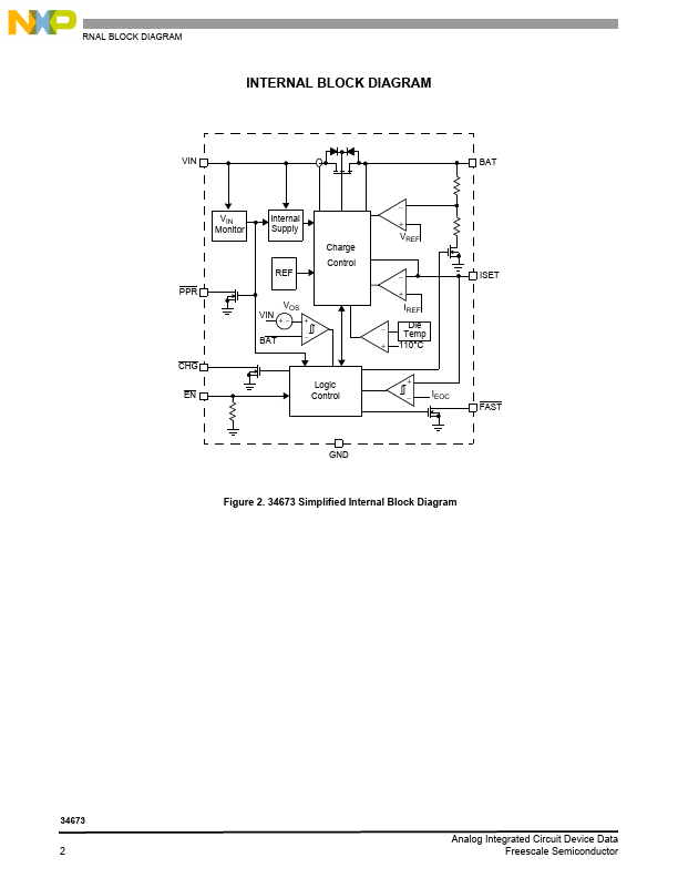
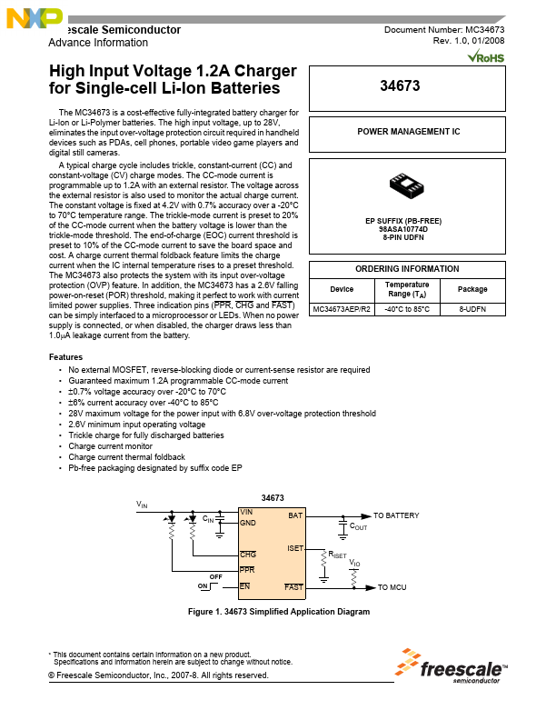
● Pb-free packaging designated by suffix code EP VIN 34673 VIN CIN GND BAT TO BATTERY COUT OFF ON CHG PPR EN ISET FAST RISET VIO TO MCU Figure 1. 34673 Simplified Application Diagram * This document contains certain information on a new product. Specifications and information herein are subject to change without notice. © Freescale Semiconductor, Inc., 2007-8. All rights reserved. INTERNAL BLOCK DIAGRAM INTERNAL BLOCK DIAGRAM VIN BAT PPR VIN Monitor Internal Supply REF VOS VIN + – + BAT – Charge Control CHG EN Logic Control – + VREF – + IREF – Die Temp + 110°C + – IEOC ISET FAST GND Figure 2.