NXP Semiconductors 34VR500
The 34VR500 is a high performance, highly integrated, multi-output, SMARTMOS, DC/DC regulator solution, with integrated power MOSFETs ideally suited for the LS1/T1 family of communication processors. Integrating four switching and five linear regulators, the 34VR500 provides power to the complete system, including the processor, DDR memory, and system peripherals.| Part No. | 34VR500 |
|---|---|
| Datasheet | 34VR500 Download |
| Manufacturer |  NXP Semiconductors |
| Description | Multi-output DC/DC regulator |
| Buy | Stock & Price |
FEATURES
:● Four buck converters:
● SW1: 4.5 A
● SW2: 2.0 A
● SW3: 2.5 A
● SW4: 1.0 A, (VTT tracking regulator)
● Five general purpose linear regulators
● DDR termination reference voltage (DDR3L and DDR4)
● Programmable low-power modes
● I2C control of all the regulators
● Power Control Logic with processor interface and event detection ES SUFFIX (WF-TYPE) 98ASA00589D 56 QFN-EP WF8X8
APPLICATIONS
:● Internet of things (IoT) gateway
● Mobile wireless router
● MFP printer
● Network attached storage
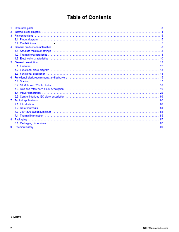
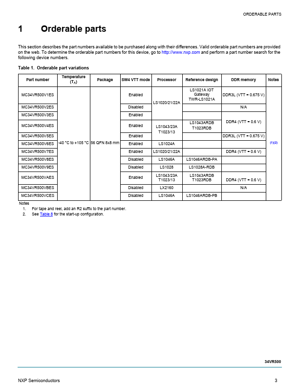
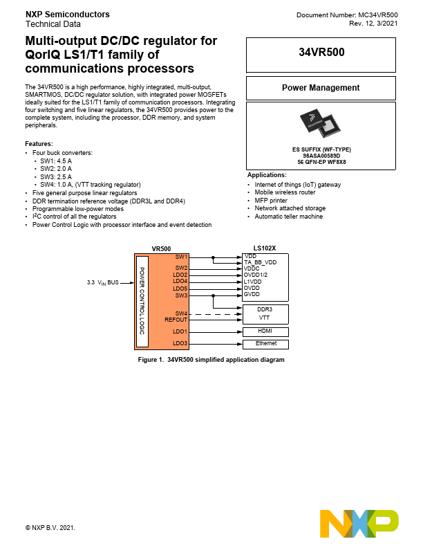
● Automatic teller machine 3.3 VIN BUS POWER CONTROL LOGIC VR500 SW1 SW2 LDO2 LDO4 LDO5 SW3 SW4 REFOUT LDO1 LDO3 LS102X VDD TA_BB_VDD VDDC OVDD1/2 L1VDD OVDD GVDD DDR3 VTT HDMI Ethernet Figure 1. 34VR500 simplified application diagram © NXP B.V. 2021. Table of Contents 1 Orderable parts . . . . . . . . . . . . . . . . . . . . . . . . . . . . . . . . . . . . . . . . . . . . . . . . . . . . . . . . . . . . . . . . . . . . . . . . . . . . . . . . . . . . . . 3 2 Internal block diagram . . . . .