DESCRIPTION
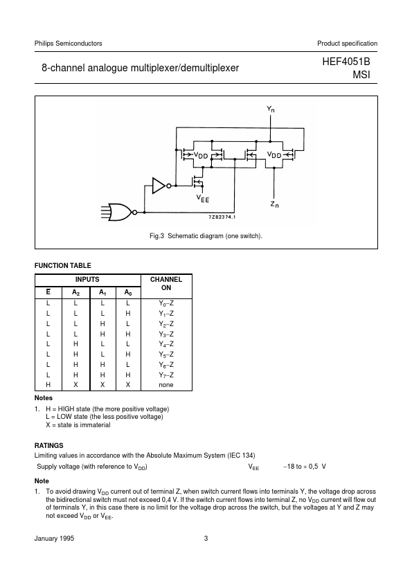
With E LOW, one of the eight switches is selected (low impedance ON-state) by A0 to A2. With E HIGH, all switches are in the high impedance OFF-state, independent of A0 to A2. VDD and VSS are the supply voltage connections for the digital control inputs (A0 to A2, and E). The VDD to VSS range is 3 to 15 V. HEF4051B MSI The analogue inputs/outputs (Y0 to Y7, and Z) can swing between VDD as a positive limit and VEE as a negative limit. VDD−VEE may not exceed 15 V. For operation as a digital multiplexer/demultiplexer, VEE is connected to VSS (typically ground). Fig.2 Pinning diagram. HEF4051BP(N): HEF4051BD(F): 16-lead DIL; plastic (SOT38-1) 16-lead DIL; ceramic (cerdip) (SOT74) 16-lead SO; plastic (SOT109-1) HEF4051BT(D): ( ): Package Designator North America PINNING Y0 to Y7 A0 to A2 E Z independent inputs/outputs address inputs enable input (active LOW) common input/output FAMILY DATA, IDD LIMITS category MSI Fig.1 Functional diagram. See Family Specifications. January 1995 2 Philips Semiconductors Product specification 8-channel analogue multiplexer/demultiplexer HEF4051B MSI Fig.3 Schematic diagram (one switch). NXP Semiconductors