NXP Semiconductors 54N06T
This product is designed and qualified for use in computing, communications, consumer and industrial applications only.| Part No. | 54N06T |
|---|---|
| Datasheet | 54N06T Download |
| Manufacturer |  NXP Semiconductors |
| Description | PHP54N06T |
| Buy | Stock & Price |
FEATURES AND BENEFITS
Low conduction losses due to low on-state resistance Suitable for thermally demanding environments due to 175 °C rating 1.3APPLICATIONS
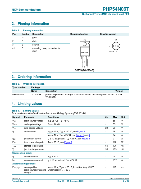
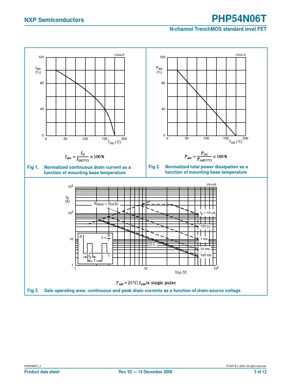
DC-to-DC convertors Switched-mode power supplies 1.4 Quick reference data Table 1. Quick reference Symbol Parameter Conditions Min Typ Max Unit VDS drain-source voltage Tj ≥ 25 °C; Tj ≤ 175 °C ID drain current Tmb = 25 °C; VGS = 10 V; see Figure 1 and 3 - - 55 V - - 54 A Ptot total power dissipation Tmb = 25 °C; see Figure 2 - - 118 W Dynamic characteristics QGD gate-drain charge VGS = 10 V; ID = 40 A; VDS = 44 V; Tj = 25 °C; see Figure 13 - 11.5 - nC Static characteristics RDSon drain-source on-state resistance VGS = 10 V; ID = 25 A; - Tj = 175 °C; see Figure 11 and 12 VGS = 10 V; ID = 25 A; Tj = 25 °C; see Figure 11 and 12 - 40 mΩ 17 20 mΩ NXP Semiconductors 2. Pinning information Table 2. Pinning information Pin SymbolDESCRIPTION
1 G gate 2 D drain 3 S source mb D mounting base; connected to drain PHP54N06T N-channel TrenchMOS standard level FET Simplified outline mb Graphic symbol D G mbb076 S 3.