FEATURES
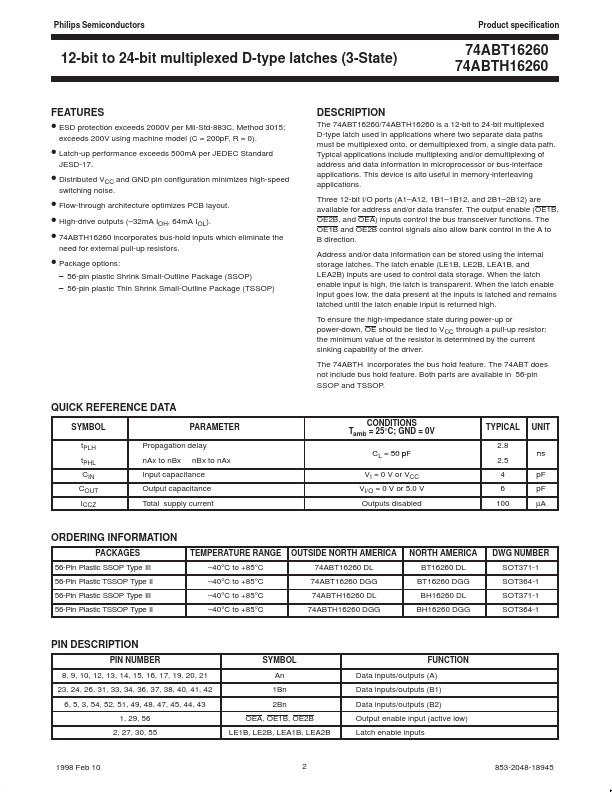
● ESD protection exceeds 2000V per Mil-Std-883C, Method 3015; exceeds 200V using machine model (C = 200pF, R = 0). DESCRIPTION
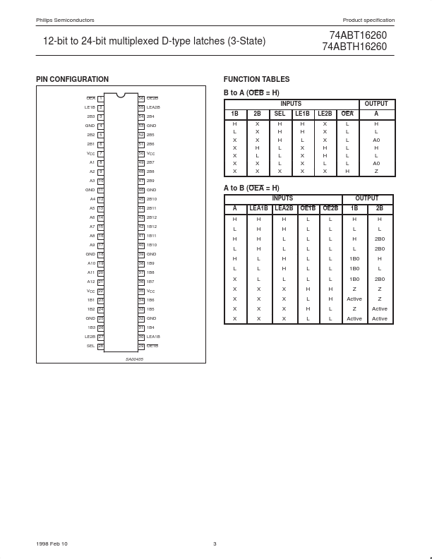
Typical applications include multiplexing and/or demultiplexing of address and data information in microprocessor or bus-interface applications. Three 12-bit I/O ports (A1–A12, 1B1–1B12, and 2B1–2B12) are available for address and/or data transfer. The OE1B and OE2B control signals also allow bank control in the A to B direction. Address and/or data information can be stored using the internal storage latches. The latch enable (LE1B, LE2B, LEA1B, and LEA2B) inputs are used to control data storage. When the latch enable input is high, the latch is transparent. When the latch enable input goes low, the data present at the inputs is latched and remains latched until the latch enable input is returned high. To ensure the high-impedance state during power-up or power-down, OE should be tied to VCC through a pull-up resistor; the minimum value of the resistor is determined by the current sinking capability of the driver. NXP Semiconductors