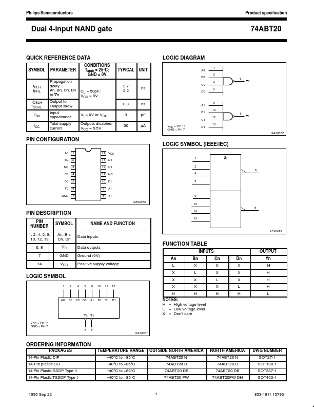
74ABT20 Overview
Key Specifications
Package: SOP
Mount Type: Surface Mount
Pins: 14
Operating Voltage: 5 V
Key Features
- 40°C to +85°C
- 40°C to +85°C
| Part | 74ABT20 |
|---|---|
| Description | Dual 4-input NAND gate |
| Manufacturer | NXP Semiconductors |
| Size | 46.01 KB |
Package: SOP
Mount Type: Surface Mount
Pins: 14
Operating Voltage: 5 V
| Seller | Inventory | Price Breaks | Buy |
|---|---|---|---|
| Verical | 1026 | 358+ : 1.0494 USD 500+ : 0.9445 USD 1000+ : 0.871 USD 10000+ : 0.7765 USD |
View Offer |
| Verical | 1140 | 358+ : 1.0494 USD 500+ : 0.9445 USD 1000+ : 0.871 USD 10000+ : 0.7765 USD |
View Offer |
| Part Number | Manufacturer | Description |
|---|---|---|
| 74ABT20PW | Nexperia | Dual 4-input NAND gate |
| 74ABT20 | Nexperia | Dual 4-input NAND gate |
| 74ABT20DB | Nexperia | Dual 4-input NAND gate |
| 74ABT20D | Nexperia | Dual 4-input NAND gate |
| 74ABT241 | Fairchild Semiconductor | Octal Buffer/Line Driver |