74ABT5074 Description
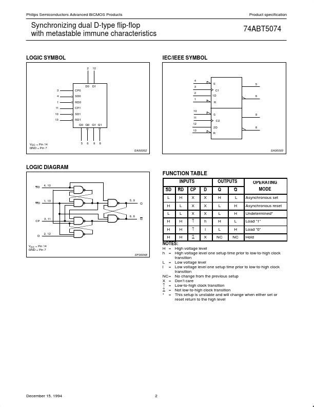
also true and plementary outputs. Set (SDn) and reset (RDn) are asynchronous active low inputs and operate independently of the clock (CPn) input. Data must be stable just one setup time prior to the low-to-high transition of the clock for guaranteed propagation delays.
74ABT5074 Key Features
- Metastable immune characteristics
- Pin patible with 74F74 and 74F5074
- Typical fMAX = 200MHz
- Output skew guaranteed less than 2.0ns
- High source current (IOH = 15mA) ideal for clock driver