Datasheet Summary
Low-power buffer/line driver; 3-state
Rev. 9
- 14 January 2022
Product data sheet
1. General description
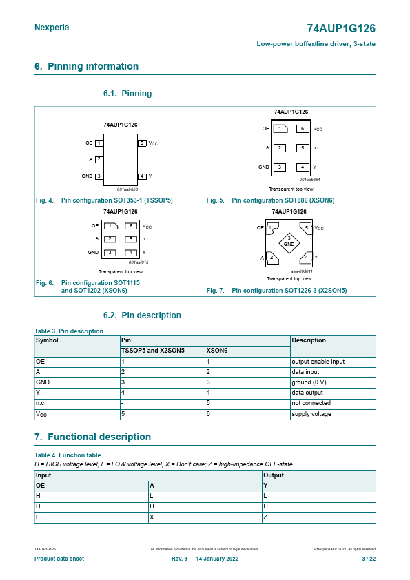
The 74AUP1G126 provides a single non-inverting buffer/line driver with 3-state output. The 3-state output is controlled by the output enable input (OE). A LOW level at pin OE causes the output to assume a high-impedance OFF-state. This device has the input-disable feature, which allows floating input signals. The inputs are disabled when the output enable input OE is LOW.
Schmitt-trigger action at all inputs makes the circuit tolerant to slower input rise and fall times across the entire VCC range from 0.8 V to 3.6 V. This device ensures a very low static and dynamic power...