NXP Semiconductors 74F175A
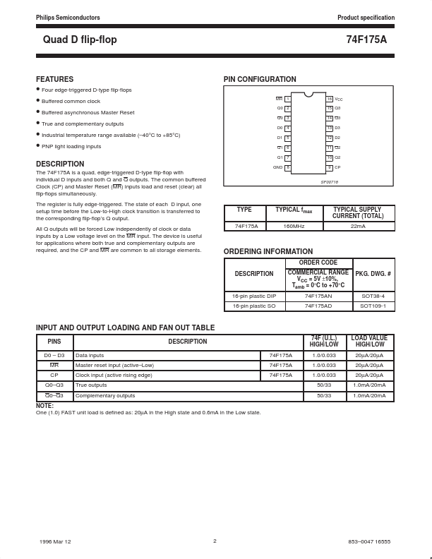
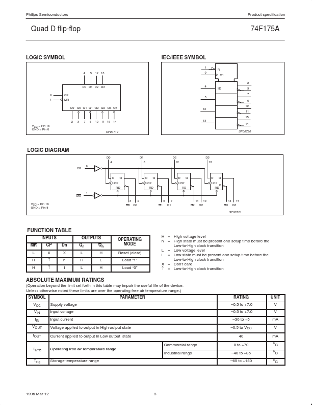
The 74F175A is a quad, edge-triggered D-type flip-flop with individual D inputs and both Q and Q outputs. The common buffered Clock (CP) and Master Reset (MR) inputs load and reset (clear) all flip-flops simultaneously. The register is fully edge-triggered.| Part No. | 74F175A |
|---|---|
| Datasheet | 74F175A Download |
| Manufacturer |  NXP Semiconductors |
| Description | Quad D flip-flop |
| Buy | Stock & Price |
FEATURES
● Four edge-triggered D-type flip-flops● Buffered common clock
● Buffered asynchronous Master Reset
● True and complementary outputs
● Industrial temperature range available (–40°C to +85°C)
● PNP light loading inputs
DESCRIPTION
The register is fully edge-triggered. The state of each D input, one setup time before the Low-to-High clock transition is transferred to the corresponding flip-flop’s Q output. All Q outputs will be forced Low independently of clock or data inputs by a Low voltage level on the MR input. The device is useful for applications where both true and complementary outputs are required, and the CP and MR are common to all storage elements. PIN CONFIGURATION MR 1 16 VCC 15 Q3 14 Q3 13 D3 12 D2 11 Q2 10 Q2 9 CP Q0 2 Q0 3 D0 4 D1 5 Q1 6 Q1 7 GND 8 SF00718 TYPE 74F175A TYPICAL fmax 160MHz TYPICAL SUPPLY CURRENT (TOTAL) 22mA ORDERING INFORMATION ORDER CODEDESCRIPTION
COMMERCIAL RANGE VCC = 5V ±10%, Tamb = 0°C to +70°C 74F175AN 74F175AD PKG. DWG. # 16-pin plasti...