NXP Semiconductors 74HC139-Q100
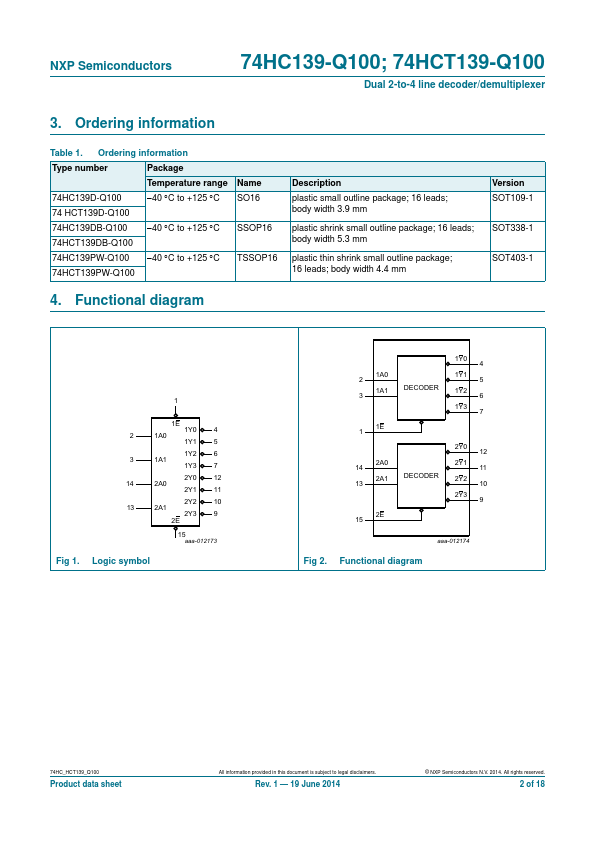
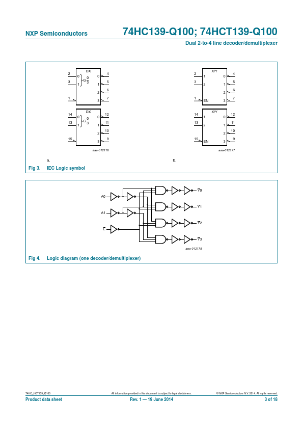
The 74HC139-Q100; 74HCT139-Q100 decodes two binary weighted address inputs (nA0, nA1) to four mutually exclusive outputs (nY0 to nY3). Each decoder features an enable input (nE). When nE is HIGH all outputs are forced HIGH.| Part No. | 74HC139-Q100 |
|---|---|
| Datasheet | 74HC139-Q100 Download |
| Manufacturer |  NXP Semiconductors |
| Description | Dual 2-to-4 line decoder/demultiplexer |
| Buy | Stock & Price |
FEATURES AND BENEFITS
● Automotive product qualification in accordance with AEC-Q100 (Grade 1)● Specified from 40 C to +85 C and from 40 C to +125 C
● Input levels:
● For 74HC139-Q100: CMOS level
● For 74HCT139-Q100: TTL level
● Demultiplexing capability
● 2 independent 2-to-4 decoders
● Multifunction capability
● Suitable for memory decoding, data routing or code conversion
● Complies with JEDEC standard no. 7A
● Active LOW mutually exclusive outputs
● ESD protection:
● MIL-STD-883, method 3015 exceeds 2000 V
● HBM JESD22-A114F exceeds 2000 V
● MM JESD22-A115-A exceeds 200 V (C = 200 pF, R = 0 )
● Multiple package options NXP Semiconductors 74HC139-Q100; 74HCT139-Q100 Dual 2-to-4 line decoder/demultiplexer 3. Ordering information Table 1. Ordering information Type number Package Temperature range Name 74HC139D-Q100 40 C to +125 C SO16 74 HCT139D-Q100 74HC139DB-Q100 40 C to +125 C SSOP16 74HCT139DB-Q100 74HC139PW-Q100 40 C to +125 C TSSOP16 74HCT139PW-Q100
DESCRIPTION
...