NXP Semiconductors 74LVC1G66
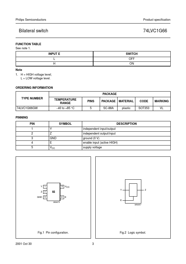
The 74LVC1G66 is a high-speed Si-gate CMOS device. The 74LVC1G66 provides an analog switch. The switch has two input/output pins (Y and Z) and an active HIGH enable input pin (E).| Part No. | 74LVC1G66 |
|---|---|
| Datasheet | 74LVC1G66 Download |
| Manufacturer |  NXP Semiconductors |
| Description | Bilateral switch |
| Buy | Stock & Price |

FEATURES
● Very low ON resistance: – 10 Ω (typical) at VCC = 2.7 V – 8 Ω (typical) at VCC = 3.3 V – 6 Ω (typical) at VCC = 5 V.● ESD protection: – HBM EIA/JESD22-A114-A exceeds 2000 V – MM EIA/JESD22-A115-A exceeds 200 V.
● High noise immunity
● CMOS low power consumption
● Latch up performance exceeds 250 mA
● SOT353 package
● Direct interface TTL-levels. QUICK REFERENCE DATA Ground = 0 V; Tamb = 25 °C; tr = tf ≤ 3.0 ns. SYMBOL tPZH/tPZL tPHZ/tPLZ CI CPD CS PARAMETER turn-on time E to Vos turn-off time E to Vos input capacitance power dissipation capacitance switch capacitance CL = 50 pF; f = 10 MHz; VCC = 3.3 V; notes 1 and 2 OFF-state ON-state Notes 1. CPD is used to determine the dynamic power dissipation (PD in µW). PD = CPD × VCC2 × fi + (CL + CS) × VCC2 × fo where: fi = input frequency in MHz; fo = output frequency in MHz; CL = output load capacitance in pF; CS = max. switch capacitance in pF; VCC = supply voltage in Volts. 2. The condition is VI = GND to VCC. CONDITIONS CL = 5...