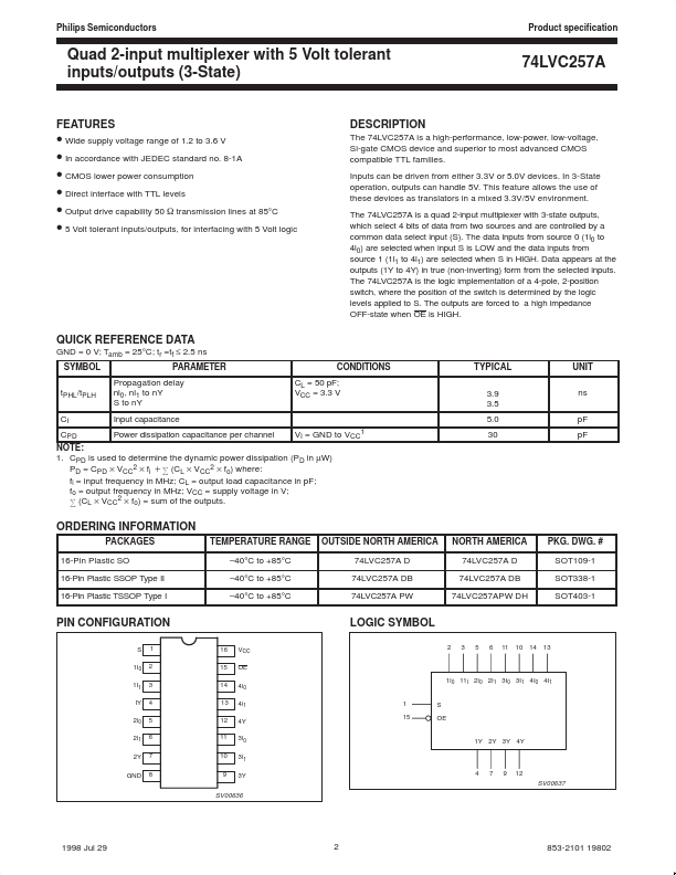
74LVC257A Description
The 74LVC257A is a high-performance, low-power, low-voltage, Si-gate CMOS device and superior to most advanced CMOS patible TTL families. Inputs can be driven from either 3.3V or 5.0V devices. In 3-State operation, outputs can handle 5V.
74LVC257A Key Features
- Wide supply voltage range of 1.2 to 3.6 V
- In accordance with JEDEC standard no. 8-1A
- CMOS lower power consumption
- Direct interface with TTL levels
- Output drive capability 50 W transmission lines at 85°C
- 5 Volt tolerant inputs/outputs, for interfacing with 5 Volt logic