NXP Semiconductors 74LVC2952A
The 74LVC2952A is a low-power, low-voltage, Si-gate CMOS device and superior to most advanced CMOS compatible TTL families. The 74LVC2952A is an octal non-inverting registered transceiver. The data is then present at the 3-State output buffers, but is only accessible when the output enable input (OEnn) is LOW.| Part No. | 74LVC2952A |
|---|---|
| Datasheet | 74LVC2952A Download |
| Manufacturer |  NXP Semiconductors |
| Description | Octal registered tranceiver |
| Buy | Stock & Price |
FEATURES
● 5-volt tolerant inputs/outputs, for interfacing with 5-volt logic● Wide supply voltage range of 1.2 V to 3.6 V
● In accordance with the JEDEC standard no. 8-1 A
● Inputs accept voltages up to 5.5 V
● CMOS low power consumption
● Flow-through pin-out architecture
● 3-State outputs
● Direct interface with TTL levels
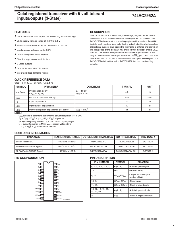
● Integrated 30W damping resistor QUICK REFERENCE DATA GND = 0 V; Tamb = 25°C; tr =tf ≤ 2.5 ns SYMBOL tPHL/tPLH fmax CI CI/O CPD PARAMETER Propagation delay CPnn to An, Bn Maximum clock frequency Input capacitance Input/output capacitance Power dissipation capacitance per buffer VCC = 3.3V1
DESCRIPTION
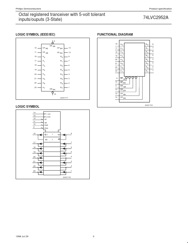
Two 8-bit back to back registers store data flowing in both directions between two bidirectional busses. Data applied to the inputs is entered and stored on the rising edge of the clock (CPnn) provided that the clock enable CEnn) is LOW. Data flow from A inputs to B outputs is the same as for B inputs to A outputs. The 74LVC2952A is identical to the 74LVC2953A but has non-inverting outputs.