NXP Semiconductors 74LVC2G00-Q100
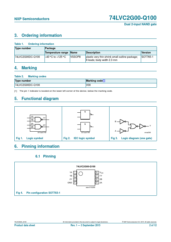
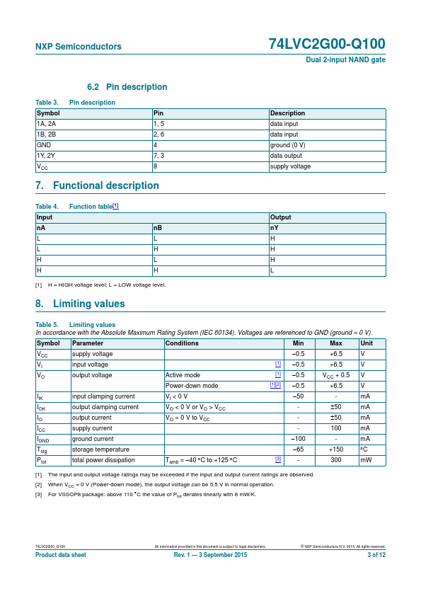
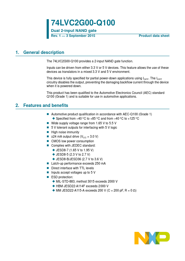
The 74LVC2G00-Q100 provides a 2-input NAND gate function. This feature allows the use of these devices as translators in a mixed 3.3 V and 5 V environment. This device is fully specified for partial power-down applications using IOFF.| Part No. | 74LVC2G00-Q100 |
|---|---|
| Datasheet | 74LVC2G00-Q100 Download |
| Manufacturer |  NXP Semiconductors |
| Description | Dual 2-input NAND gate |
| Buy | Stock & Price |
FEATURES AND BENEFITS
● Automotive product qualification in accordance with AEC-Q100 (Grade 1)● Specified from 40 C to +85 C and from 40 C to +125 C
● Wide supply voltage range from 1.65 V to 5.5 V
● 5 V tolerant outputs for interfacing with 5 V logic
● High noise immunity
● 24 mA output drive (VCC = 3.0 V)
● CMOS low power consumption
● Complies with JEDEC standard:
● JESD8-7 (1.65 V to 1.95 V)
● JESD8-5 (2.3 V to 2.7 V)
● JESD8-B/JESD36 (2.7 V to 3.6 V)
● Latch-up performance exceeds 250 mA
● Direct interface with TTL levels
● Inputs accept voltages up to 5 V
● ESD protection:
● MIL-STD-883, method 3015 exceeds 2000 V
● HBM JESD22-A114F exceeds 2000 V
● MM JESD22-A115-A exceeds 200 V (C = 200 pF, R = 0 ) NXP Semiconductors 74LVC2G00-Q100 Dual 2-input NAND gate 3. Ordering information Table 1. Ordering information Type number Package Temperature range Name 74LVC2G00DC-Q100 40 C to +125 C VSSOP8
DESCRIPTION
plastic very thin shrink small outline package; 8 leads; body width 2.3 mm Version SOT765-1 4.