Datasheet4U Logo Datasheet4U.com

74LVC3G14 - Triple inverting Schmitt trigger

General Description

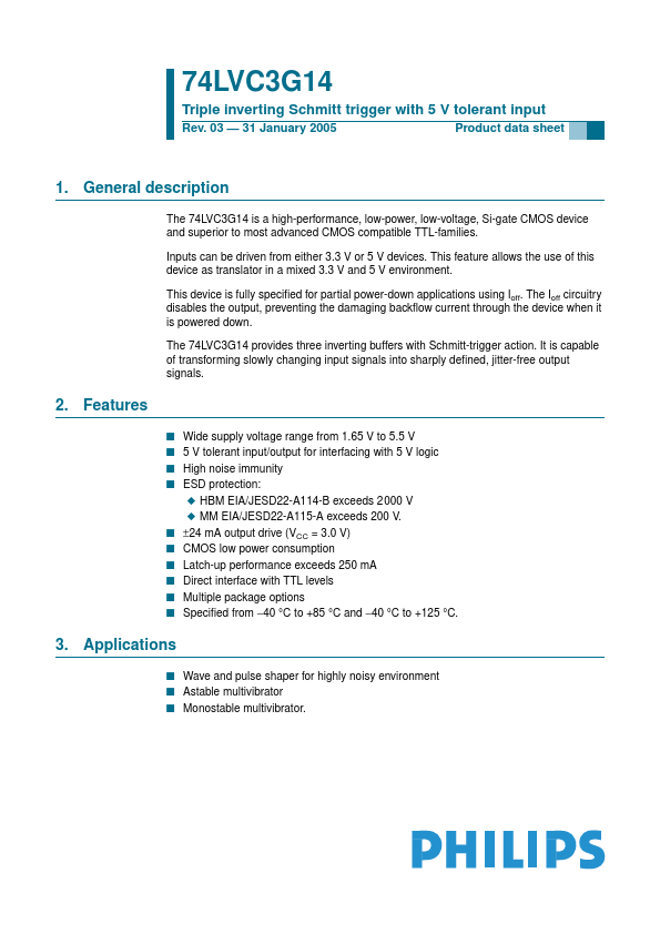
The 74LVC3G14 is a high-performance, low-power, low-voltage, Si-gate CMOS device and superior to most advanced CMOS compatible TTL-families.

Inputs can be driven from either 3.3 V or 5 V devices.

This feature allows the use of this device as translator in a mixed 3.3 V and 5 V environment.

Key Features

  • s s s s Wide supply voltage range from 1.65 V to 5.5 V 5 V tolerant input/output for interfacing with 5 V logic High noise immunity ESD protection: x HBM EIA/JESD22-A114-B exceeds 2000 V x MM EIA/JESD22-A115-A exceeds 200 V. ±24 mA output drive (VCC = 3.0 V) CMOS low power consumption Latch-up performance exceeds 250 mA Direct interface with TTL levels Multiple package options Specified from.
  • 40 °C to +85 °C and.
  • 40 °C to +125 °C. s s s s s s 3.

📥 Download Datasheet

Full PDF Text Transcription (Reference)

The following content is an automatically extracted verbatim text from the original manufacturer datasheet and is provided for reference purposes only.

View original datasheet text
74LVC3G14 Triple inverting Schmitt trigger with 5 V tolerant input Rev. 03 — 31 January 2005 Product data sheet 1. General description The 74LVC3G14 is a high-performance, low-power, low-voltage, Si-gate CMOS device and superior to most advanced CMOS compatible TTL-families. Inputs can be driven from either 3.3 V or 5 V devices. This feature allows the use of this device as translator in a mixed 3.3 V and 5 V environment. This device is fully specified for partial power-down applications using Ioff. The Ioff circuitry disables the output, preventing the damaging backflow current through the device when it is powered down. The 74LVC3G14 provides three inverting buffers with Schmitt-trigger action.