NXP Semiconductors 74LVC821A
The 74LVC821A is a high performance, low-power, low-voltage Si-gate CMOS device and superior to most advanced CMOS compatible TTL families. This feature allows the use of these devices as translators in a mixed 3.3V/5V environment. The 74LVC821A is a10-bit D-type flip-flop featuring separate D-type inputs for each flip-flop and 3-State outputs for bus-oriented applications.| Part No. | 74LVC821A |
|---|---|
| Datasheet | 74LVC821A Download |
| Manufacturer |  NXP Semiconductors |
| Description | 10-bit D-type flip-flop |
| Buy | Stock & Price |

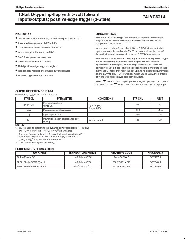
FEATURES
● 5-volt tolerant inputs/outputs, for interfacing with 5-volt logic● Supply voltage range of 2.7V to 3.6V
● Complies with JEDEC standard no. 8-1A
● Inputs accept voltages up to 5.5V
● CMOS low power consumption
● Direct interface with TTL levels
● 10-bit positive edge-triggered register
● Independent register and 3-State buffer operation
● Flow-through pin-out architecture
DESCRIPTION
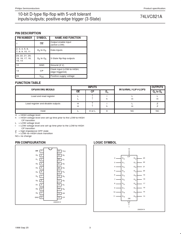
Inputs can be driven from either 3.3V or 5.0V devices. In 3-state operation, outputs can handle 5V. A clock (CP) and an output enable (OE) input are common to all flip-flops. The ten flip-flops will store the state of their individual D-inputs that meet the set-up and hold times requirements on the LOW-to-HIGH CP transition. When OE is LOW, the contents of the ten flip-flops is available at the outputs. When OE is HIGH, the outputs go to the high impedance OFF-state. Operation of the OE input does not affect the state of the flip-flops. QUICK REFERENCE DATA GND = 0 V; Tamb = 25°C; tr = tf ≤ 2.5...