NXP Semiconductors ADC0820
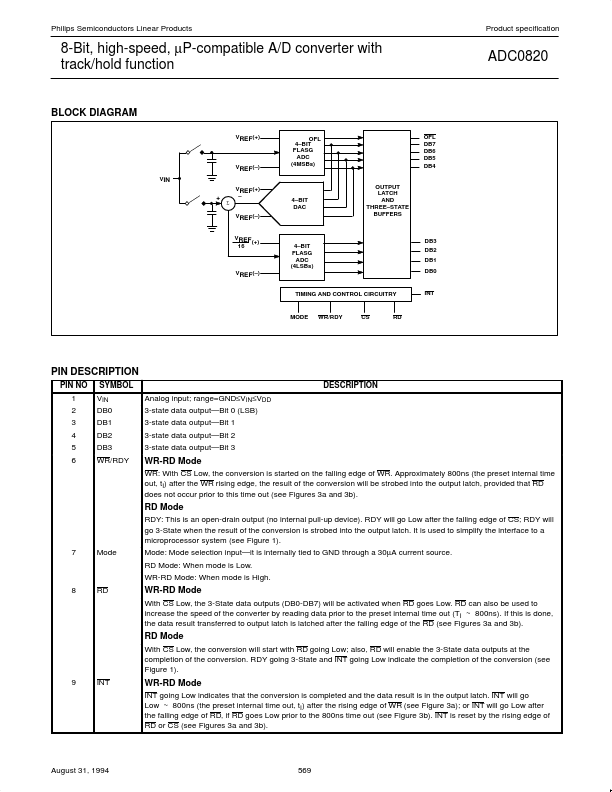
the ADC0820 is tracked and held by the input sampling circuitry, eliminating the need for an external sample-and-hold for signals slewing at less than 100mV/µs. For ease of interface to microprocessors, the ADC0820 has been designed to appear as a memory location or I/O port without the need for external interfacing logic.| Part No. | ADC0820 |
|---|---|
| Datasheet | ADC0820 Download |
| Manufacturer |  NXP Semiconductors |
| Description | A/D converter |
| Buy | Stock & Price |
DESCRIPTION
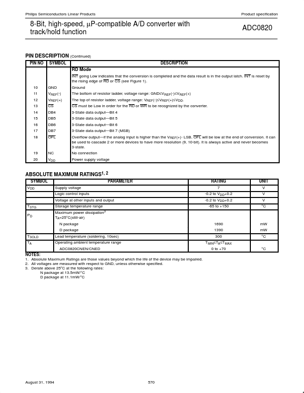
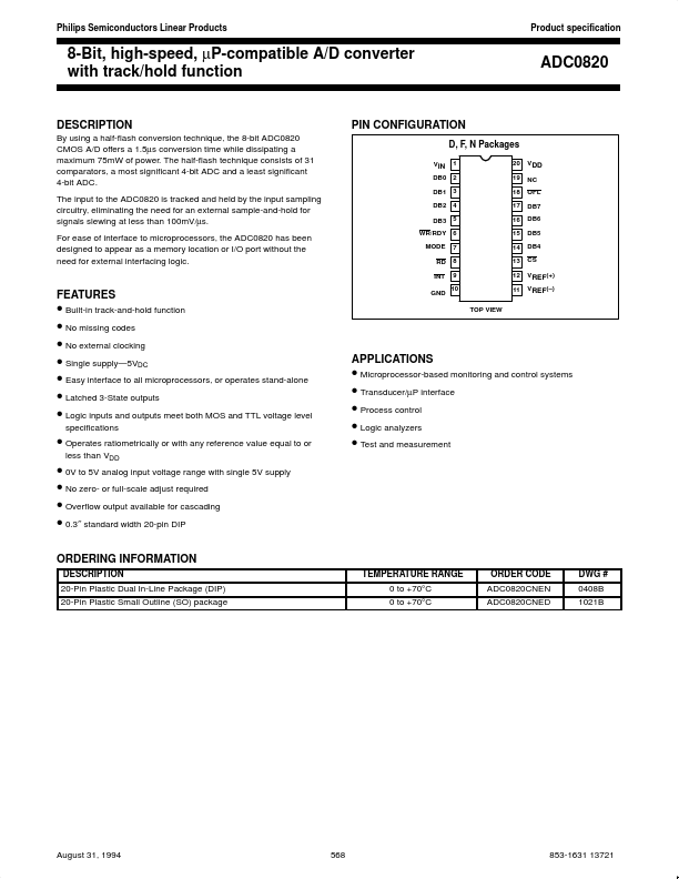
By using a half-flash conversion technique, the 8-bit ADC0820 CMOS A/D offers a 1.5µs conversion time while dissipating a maximum 75mW of power. The half-flash technique consists of 31 comparators, a most significant 4-bit ADC and a least significant 4-bit ADC. The input to PIN CONFIGURATION D, F, N Packages VIN 1 20 19 18 17 16 15 14 13 12 11 TOP VIEW VDD NC OFL DB7 DB6 DB5 DB4 CS VREF(+) VREF(–) DB0 2 DB1 3 DB2 4 DB3 5 WR/RDY MODE RD INT 6 7 8 9 10FEATURES
GND● Built-in track-and-hold function
● No missing codes
● No external clocking
● Single supply—5VDC
● Easy interface to all microprocessors, or operates stand-alone
● Latched 3-State outputs
● Logic inputs and outputs meet both MOS and TTL voltage level specifications
APPLICATIONS
● Operates ratiometrically or with any reference value equal to or● 0V to 5V analog input voltage range with single 5V supply
● No zero- or full-scale adjust required
● Overflow output available for cascading
● 0.3″ standard width 20-pin D...