FEATURES AND BENEFITS
SNR, 70 dBFS; SFDR, 86 dBc Sample rate up to 125 Msps 12-bit pipelined ADC core Clock input divider by 2 for less jitter contribution Single 3 V supply Flexible input voltage range: 1 V p-p to 2 V p-p CMOS or LVDS DDR digital outputs Pin compatible with the ADC1410S series and the ADC1010 series HVQFN40 package Input bandwidth, 600 MHz Power dissipation, 430 mW at 80 Msps Serial Peripheral Interface (SPI) Duty cycle stabilizer Fast OuT of Range (OTR) detection INL ±0.25 LSB, DNL ±0.12 LSB Offset binary, two’s complement, gray code Power-down and Sleep modes 3. APPLICATIONS
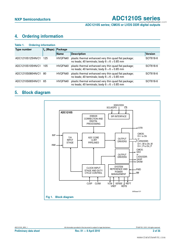
Wireless and wired broadband communications Spectral analysis Ultrasound equipment Portable instrumentation Imaging systems Software define radio NXP Semiconductors ADC1210S series ADC1210S series; CMOS or LVDS DDR digital outputs 4. Ordering information Table 1. Ordering information fs (Msps) Package Name ADC1210S125HN/C1 125 ADC1210S105HN/C1 105 AD... NXP Semiconductors