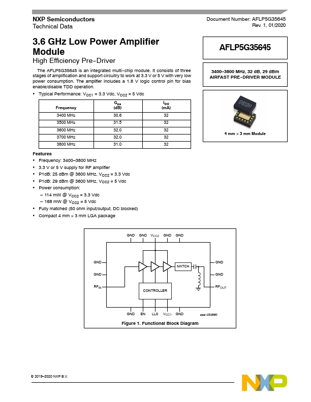
AFLP5G35645 Description
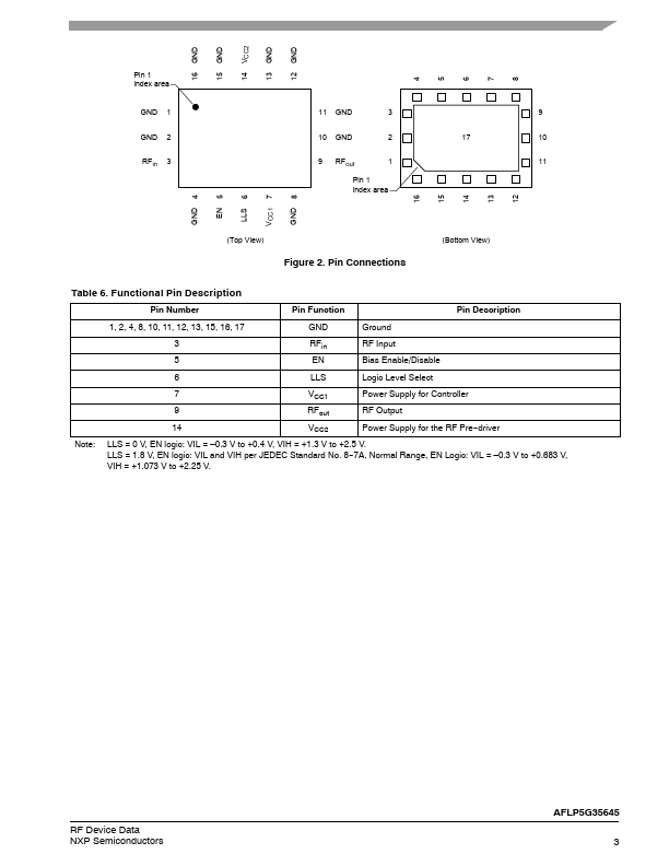
7 VCC1 Power Supply for Controller 9 RFout RF Output 14 VCC2 Power Supply.
AFLP5G35645 Key Features
- Frequency: 3400-3800 MHz
- 3.3 V or 5 V supply for RF amplifier
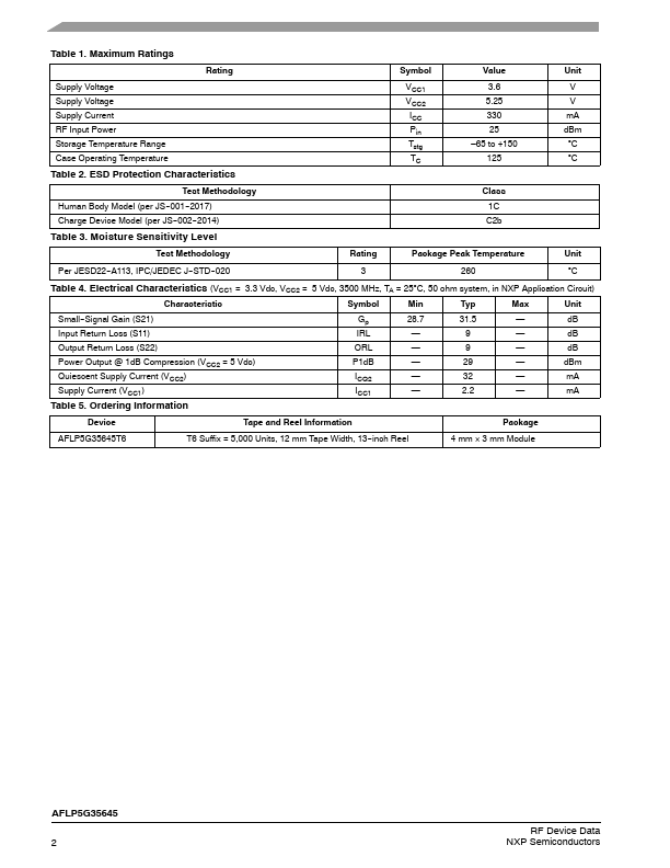
- P1dB: 25 dBm @ 3600 MHz, VCC2 = 3.3 Vdc
- P1dB: 29 dBm @ 3600 MHz, VCC2 = 5 Vdc
- Power consumption
- 114 mW @ VCC2 = 3.3 Vdc
- 168 mW @ VCC2 = 5 Vdc
- Fully matched (50 ohm input/output, DC blocked)
- pact 4 mm 3 mm LGA package