AV162827DGG Description
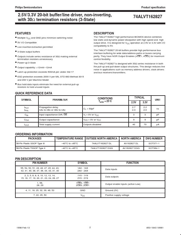
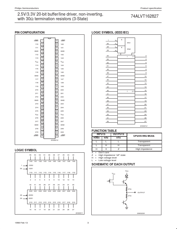
74ALVT162827 Multiple VCC and GND pins minimize switching noise 5V I/O patible Live insertion/extraction permitted 3-State output buffers Outputs include series resistance of 30Ω making external Power-up 3-State Output capability: +12mA/ 12mA Latch-up protection exceeds 500mA per Jedec Std 17 ESD protection exceeds 2000 V per MIL STD 883 Method 3015 and 200 V per Machine Model termination resistors unnecessary The...
AV162827DGG Key Features
- Multiple VCC and GND pins minimize switching noise
- 5V I/O patible
- Live insertion/extraction permitted
- 3-State output buffers
- Outputs include series resistance of 30Ω making external
- Power-up 3-State
- Output capability: +12mA/-12mA
- Latch-up protection exceeds 500mA per Jedec Std 17
- ESD protection exceeds 2000 V per MIL STD 883 Method 3015
AV162827DGG Applications
- Bus hold data inputs eliminate the need for external pull-up