DESCRIPTION
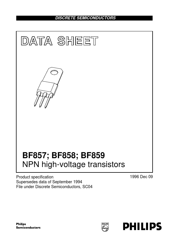
NPN transistors in a TO-202 plastic package. An A-version with e-b-c pinning instead of e-c-b is available on request. APPLICATIONS
● For use in video output stages of black and white and colour television receivers. PINNING PIN DESCRIPTION
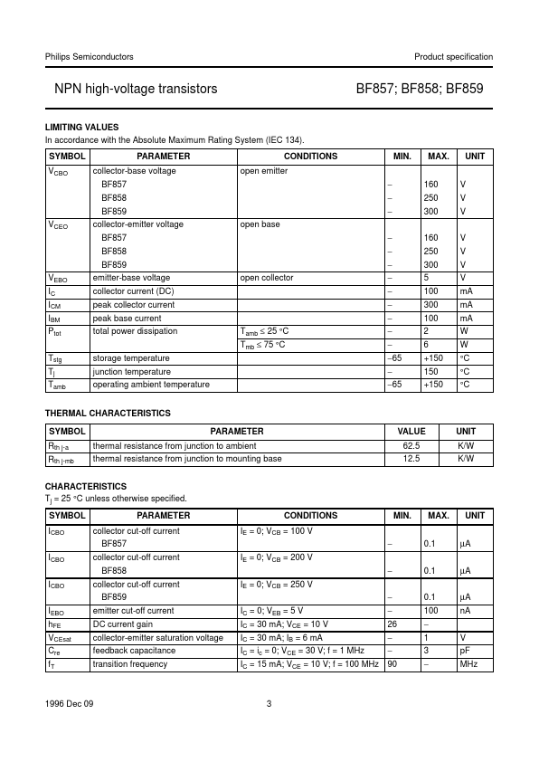
1 emitter 2 collector, connected to mounting base 3 base handbook, halfpage 1 23 MBH794 Fig.1 Simplified outline (TO-202) and symbol. QUICK REFERENCE DATA SYMBOL PARAMETER VCBO collector-base voltage BF857 BF858 BF859 VCEO collector-emitter voltage BF857 BF858 BF859 ICM peak collector current Ptot total power dissipation hFE DC current gain Cre feedback capacitance fT transition frequency CONDITIONS open emitter open base Tmb ≤ 75 °C IC = 30 mA; VCE = 10 V IC = ic = 0; VCE = 30 V; f = 1 MHz IC = 15 mA; VCE = 10 V; f = 100 MHz MIN. MAX. UNIT − 160 V − 250 V − 300 V − 160 V − 250 V − 300 V − 300 mA −6W 26 − − 3 pF 90 − MHz 1996 Dec 09 2 Philips Semiconductors NPN high-voltage transistors Product specification BF857; BF858; BF859 LIMITING VALUES In accordance with the Absolute Maximum Rating System (IEC 134). NXP Semiconductors