NXP Semiconductors BSH103
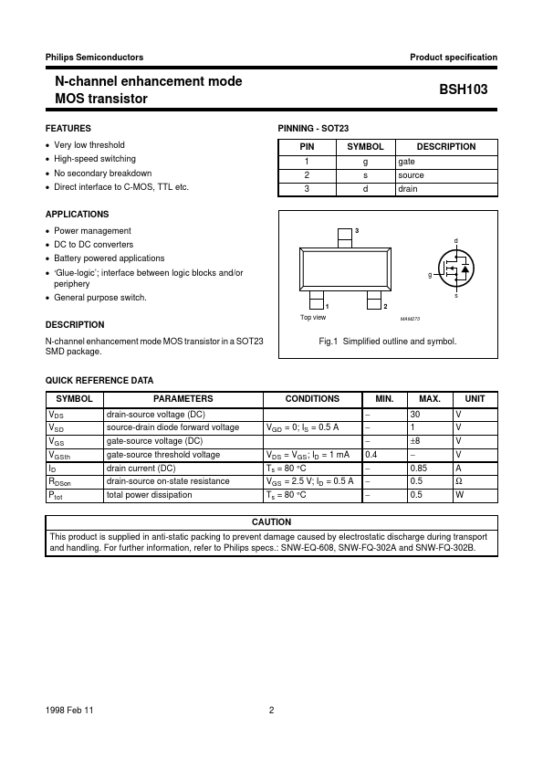
This product is supplied in anti-static packing to prevent damage caused by electrostatic discharge during transport and handling. For further information, refer to Philips specs.: SNW-EQ-608, SNW-FQ-302A and SNW-FQ-302B.BSH103 Specifications
- Package : SOT-23
- Threshold Voltage : 400mV
- Drain-Source Resistance : 500mΩ
- Drain-Source Voltage : 30V
- Terminals : 3
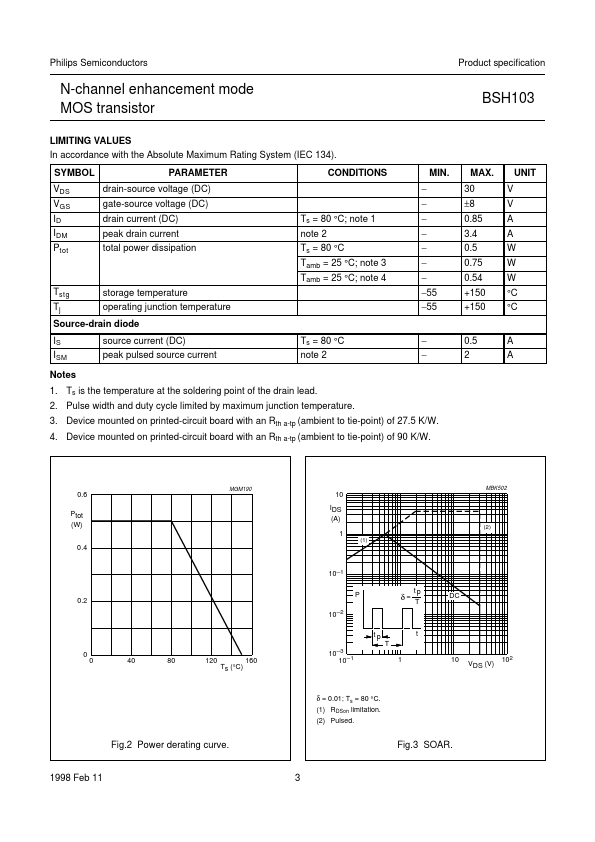
- Max Power Dissipation : 750mW
- Termination : SMD/SMT
- Max Operating Temp : 150°C
- Min Operating Temp : -55°C
Source:
Octopart
| Part No. | BSH103 |
|---|---|
| Datasheet | BSH103 Download |
| Manufacturer |  NXP Semiconductors |
| Description | N-channel enhancement mode MOS transistor |
| Buy | Stock & Price |
FEATURES
● Very low threshold● High-speed switching
● No secondary breakdown
● Direct interface to C-MOS, TTL etc.
APPLICATIONS
● Power management● DC to DC converters
● Battery powered applications
● ‘Glue-logic’; interface between logic blocks and/or periphery
● General purpose switch. 1 Top view 2 MAM273 BSH103 PINNING - SOT23 PIN 1 2 3 SYMBOL g s d gate source drain
DESCRIPTION
handbook, halfpage 3 d g sDESCRIPTION
N-channel enhancement mode MOS transistor in a SOT23 SMD package. QUICK REFERENCE DATA SYMBOL VDS VSD VGS VGSth ID RDSon Ptot PARAMETERS drain-source voltage (DC) source-drain diode forward voltage gate-source voltage (DC) gate-source threshold voltage drain current (DC) drain-source on-state resistance total power dissipation VDS = VGS ; ID = 1 mA Ts = 80 °C VGS = 2.5 V; ID = 0.5 A Ts = 80 °C CAUTION VGD = 0; IS = 0.5 A CONDITIONS − − − 0.4 − − − MIN. Fig.1 Simplified outline and symbol. MAX. 30 1 ±8 − 0.85 0.5 0.5 V V V V A Ω W UNIT 1998 Feb 11 2 Philips Semiconductors Product specification N-channel enhancement mode MOS transistor LIMITING VALUES In accordance with the Absolute Maximum Rating System (IEC 134).