GENERAL DESCRIPTION
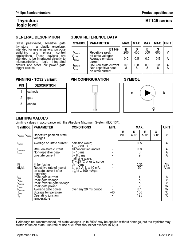
Glass passivated, sensitive gate thyristors in a plastic envelope, intended for use in general purpose switching and phase control applications. These devices are intended to be interfaced directly to microcontrollers, logic integrated circuits and other low power gate trigger circuits. BT149 series QUICK REFERENCE DATA SYMBOL VDRM, VRRM IT(AV) IT(RMS) ITSM PARAMETER BT149 Repetitive peak off-state voltages Average on-state current RMS on-state current Non-repetitive peak on-state current MAX. MAX. MAX. MAX. UNIT B 200 0.5 0.8 8 D 400 0.5 0.8 8 E 500 0.5 0.8 8 G 600 0.5 0.8 8 V A A A PINNING - TO92 variant PIN 1 2 3 DESCRIPTION
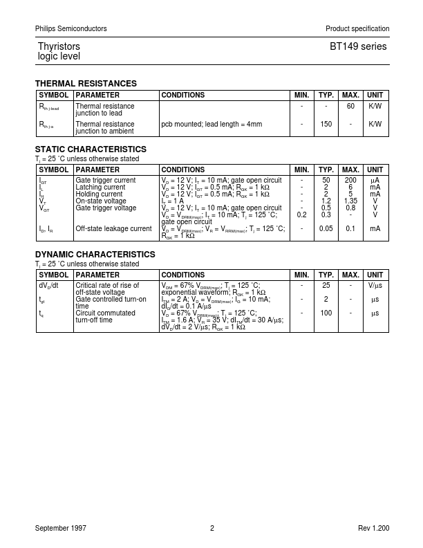
cathode gate anode PIN CONFIGURATION SYMBOL a k 3 2 1 g LIMITING VALUES Limiting values in accordance with the Absolute Maximum System (IEC 134). SYMBOL PARAMETER CONDITIONS MIN. half sine wave; Tlead ≤ 83 ˚C all conduction angles t = 10 ms t = 8.3 ms half sine wave; Tj = 25 ˚C prior to surge t = 10 ms ITM = 2 A; IG = 10 mA; dIG/dt = 100 mA/µs -40 B 2001 MAX. NXP Semiconductors