BUK107-50DS
BUK107-50DS is PowerMOS transistor Logic level TOPFET manufactured by NXP Semiconductors.
DESCRIPTION
Monolithic overload protected logic level power MOSFET in a surface mount plastic envelope, intended as a general purpose switch for automotive systems and other applications.
QUICK REFERENCE DATA
SYMBOL VDS ID PD Tj RDS(ON) PARAMETER Continuous drain source voltage Continuous drain current Total power dissipation Continuous junction temperature Drain-source on-state resistance MAX. 50 0.7 1.8 150 175 UNIT V A W ˚C mΩ
APPLICATIONS
General controller for driving lamps small motors solenoids
FEATURES
Vertical power DMOS output stage Overload protected up to 85˚C ambient Overload protection by current limiting and overtemperature sensing Latched overload protection reset by input Input clamping suitable for pull-up resistor drive circuit Control of power MOSFET and supply of overload protection circuits derived from input ESD protection on all pins Overvoltage clamping for turn off of inductive loads
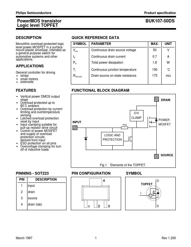
FUNCTIONAL BLOCK DIAGRAM
DRAIN
O/V CLAMP INPUT
POWER MOSFET
LOGIC AND PROTECTION
SOURCE
Fig.1. Elements of the TOPFET.
PINNING
- SOT223
PIN 1 2 3 4 input drain source drain (tab) DESCRIPTION
PIN CONFIGURATION
SYMBOL
D TOPFET I
March 1997
Rev 1.200
Philips Semiconductors
Product specification
Power MOS transistor Logic level TOPFET
LIMITING VALUES
Limiting values in accordance with the Absolute Maximum System (IEC 134) SYMBOL VDS ID II IIRM PD Tstg Tj PARAMETER Continuous drain source voltage Continuous drain current2 Continuous input current Non-repetitive peak input current Total power dissipation Storage temperature Continuous junction temperature
CONDITIONS clamping tp ≤ 1 ms Tamb = 25 ˚C normal operation3
MIN. -55
- MAX. 50 self limiting 3 10 1.8 150 150
UNIT V A m A m A W ˚C ˚C
ESD LIMITING VALUE
SYMBOL VC PARAMETER Electrostatic discharge capacitor voltage CONDITIONS Human body model; C = 250 p F; R = 1.5 kΩ MIN. MAX. 2 UNIT k V
OVERVOLTAGE CLAMPING LIMITING VALUES
At a drain source...