BUK563-48C
BUK563-48C is PowerMOS transistor Voltage clamped logic level FET manufactured by NXP Semiconductors.
DESCRIPTION
Protected N-channel enhancement mode logic level field-effect power transistor in a plastic envelope suitable for surface mount applications. The device is intended for use in automotive applications. It has built-in zener diodes providing active drain voltage clamping.
QUICK REFERENCE DATA
SYMBOL V(CL)DSR ID Ptot Tj WDSRR RDS(ON) PARAMETER Drain-source clamp voltage Drain current (DC) Total power dissipation Junction temperature Repetitive clamped turn off energy; Tj = 150˚C Drain-source on-state resistance; VGS = 5 V MIN. 40 TYP. 48 MAX. UNIT 58 21 75 175 50 85 V A W ˚C m J mΩ
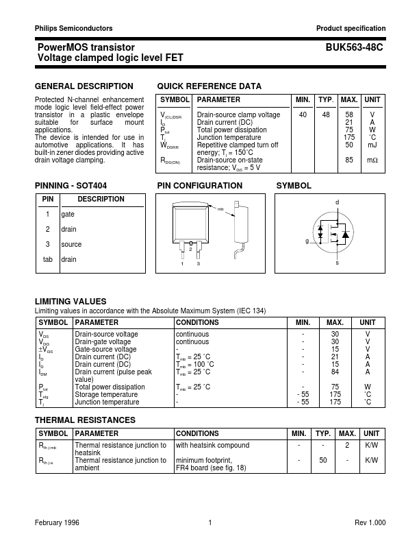
PINNING
- SOT404
PIN 1 2 3 tab gate drain source drain DESCRIPTION
PIN CONFIGURATION mb
SYMBOL d g
2 1 3 s
LIMITING VALUES
Limiting values in accordance with the Absolute Maximum System (IEC 134) SYMBOL VDS VDG ±VGS ID ID IDM Ptot Tstg Tj PARAMETER Drain-source voltage Drain-gate voltage Gate-source voltage Drain current (DC) Drain current (DC) Drain current (pulse peak value) Total power dissipation Storage temperature Junction temperature CONDITIONS continuous continuous Tmb = 25 ˚C Tmb = 100 ˚C Tmb = 25 ˚C Tmb = 25 ˚C MIN.
- 55
- 55 MAX. 30 30 15 21 15 84 75 175 175 UNIT V V V A A A W ˚C ˚C
THERMAL RESISTANCES
SYMBOL Rth j-mb Rth j-a PARAMETER Thermal resistance junction to heatsink Thermal resistance junction to ambient CONDITIONS with heatsink pound minimum footprint, FR4 board (see fig. 18) MIN. TYP. 50 MAX. 2 UNIT K/W K/W
February 1996
Rev 1.000
Philips Semiconductors
Product specification
Power MOS transistor Voltage clamped logic level FET
STATIC CHARACTERISTICS
Tj = 25 ˚C unless otherwise specified SYMBOL V(BR)DG VGS(TO) VGS(ON) IDSS IGSS RDS(ON) PARAMETER Drain-gate zener voltage Gate threshold voltage Gate voltage Zero gate voltage drain current Gate source leakage current Drain-source on-state resistance CONDITIONS 0.2 < -IG < 0.4 m A; -55˚C < Tj < 150˚C VDS = VGS; ID = 1 m A VDS = 10 V; ID = 10 A; -55˚C < Tj < 150˚C VDS = 30 V; VGS = 0 V; Tj...